Appendix A. I/F Specifications
120
November 2001
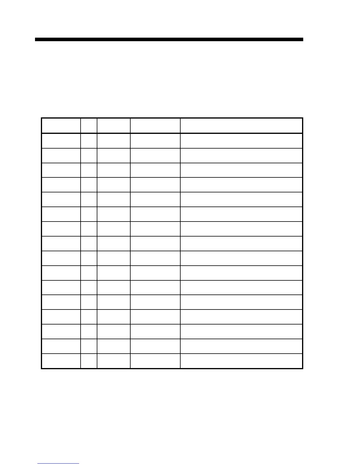
A.3 V.35 User Data Channel Connector
When the ETU-01A is ordered with a V.35 interface, the
physical interface is a 34-pin female M-Block type connector
wired in accordance with Table A-4.
SIGNAL
FUNCTION
PIN CIRCUIT DIRECTION DESCRIPTION
Protective
Ground
A Frame
↔↔
Chassis ground.
May be isolated from signal ground.
Signal
Ground
B
Signal
Ground
↔↔
Common signal ground.
Transmitted
Data
P
S
TD(A)
TD(B)
To ETU-01A Serial digital data from DTE.
Received
Data
R
T
RD(A)
RD(B)
From ETU-01A
Serial digital data at the output of the ETU-01A
receiver.
Request to
Sent
C
RTS
To ETU-01A
An ON signal to the ETU-01A when data
transmission is desired.
Clear to
Sent
D
CTS
From ETU-01A Constantly ON.
Data Set
Ready
E
DSR
From ETU-01A
Constantly ON,
except during test loops.
Data Terminal
Ready
H
DTR
To ETU-01A Not used.
Data Carrier
Detect
F DCD From ETU-01A
Constantly ON, except when a loss of the received
carrier signal is detected.
External
Transmit clock
U
W
ETC(A)
ETC(B)
To ETU-01A
A transmitted data rate clock input from the data
source.
Transmit
Clock
Y
AA
TC(A)
TC(B)
From ETU-01A
A transmitted data rate clock for use by an external
data source.
Receive
Clock
V
X
RC(A)
RC(B)
From ETU-01A
A received data rate clock for use by an external
data source.
External
Receive clock
Z
BB
ERC(A)
ERC(B)
To ETU-01A
A received serial data rate clock input from the
DTE.
Remote
Loop back
HH RL To ETU-01A
When on, commands ETU-01A into remote loop
back, can disable by DIP sw.
Local
Loop back
JJ LL To ETU-01A
When on, commands ETU-01A into local loop
back, can disable by DIP sw.
Test Indicator KK TM From ETU-01A ON during any test mode
Table A-4 V.35 user data channel connector pin allocation
 Loading...