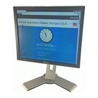
Service Manual
monitors VBUS_DET to determine when to assert the internal
D+ pull-up resistor.
53
VSS Ground
54
VDD18 +1.8V core power
55
VSS Ground
56
NC Not connected
57
XTAL2 OCLKx 24MHz crystal
This is the other terminal of the crystal, or left unconnected when
an external clock source is used to drive XTAL1/CLKIN.
58
XTAL/CLKIN 24MHz crystal or external clock input.
59
CFG/-SEL2 I This pin is read on the rising edge of RESET_N negation and
will determine the hub configuration method.
60
VDDA18PLL +1.8V Filtered analog power for internal PLL.
61
VDDA33PLL +3.3V Filtered analog power for the internal PLL
62
ATEST/REG_EN AIO This signal is used for testing. The analog section of the chip,
and to enable or disable the internal 1.8v regulator.
63
RBLAS I-R A 12.0kohm (+/-1%) resistor is attached from ground to this pin
to set the transceiver’s internal bias settings.
64
VSS Ground
12.3 U850 (SG6841, PWM Power Controller)
Pin Symbol I/O Description
1 GND Ground
2 FB I Feedback, the FB pin provides the information of
the regulation. The PWM duty cycle is controlled by
FB
3 VIN I Start-up current input
4 RI I Reference setting, typical voltage 1.3V
5 RT N.C.(not connected)
6 SENSE I Current sense for over current protection
7 VDD I Power supply
8 GATE O PWM output
12.4 U1 (OZ9936G, CCFL Inverter controller IC)
Pin Symbol I/O Description
1 SST_CMP I Enable, soft start time and compensation of current
error amplifier
2 CT I Timing capacitor to set operating frequency
3 GNDA Ground
4 DRV2 O N MOSFET Driver output
5 DRV1 O N MOSFET Driver output
6 VDDA I Supply voltage input
7 VSEN_DIM I Voltage sense, input analog signal for PWM driving
control
8 ISEN I Lamp current detection & control