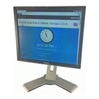
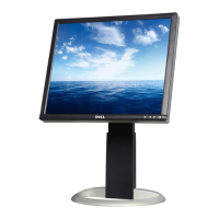
Service Manual
U401 #115 (LBADC control Pin ) is defined as “DOWN”.
- Button “Menu” on front bezel connects to U401 (gm5621-LF) #113 through CN401 #6 via R427,
U401 #113 ((LBADC control Pin ) is defined as “Menu”.
Button “Select” on front bezel connects to U401 (gm5621-LF) #113 through CN401 #7 via R428,
U401 #113 (LBADC control Pin ) is defined as “Select”.
- LED Indicator on Front Bezel
a. When press button “power”, U401(Scalar) #125 be send in low potential, make U401#51 sends out
high potential through CN401 #3 via R406 to J1#3 on keypad, LED Green on.
b. When in “Suspend” mode, U401 (Scalar) #57 sends out a high potential through CN401 #2 via
R404 to J1#2 on keypad .LED Amber ON.
2.3.4 GENESIS CHIP U401 (gm2621-LF)
- U401 (gm5621-LF) #7~#16. #31~#40 output 8 bit even LVDS digital data to panel control circuit
through CN501.
- U401 (gm5621-LF) #127 output PPWR ”H” potential to make Q502 conducted, and then make Q501
conducted, +5V flow to CN501#1~#3 as Panel Vdd .
- U401 (gm5621-LF) #49 output CCFL_ON/OFF ”H” potential to control Inverter on/off.
- U401 (gm5621-LF) #50 outputs Brightness “PWM” signals to control CCFL brightness.
- TCLK by Crystal 14.318MHz input to U401 (gm5621-LF) #109.
- U401 (gm5621-LF) #111 Bidirectional RESET signals
Please refer to gm5621-LF Pin Assignments table in page
2.3.5 Regulator Circuit
-- +5V is from power supply for U301, U302, U601,U902, U904, U905 and Panel used.
- +3.3V is from switching mode power supply for U401,U402, U404,U901,U903
- +1.8V generates from +3.3V through C603 filtering and U602 which is output +1.8V LDO, for U401
used.
2.3.6 USB circuit
- USB Signal input D+,D- through P901,#3,#2, then enter into U901 (SMSC2504) Signal input
terminal #2,#3, and then SMSC2504 deals with signal internally.
- U901 (SMSC2504) #5,#6, #8,#9 output DD+[1],DD-[1], DD+[2],DD-[2] USB data through P902
#6,#7,#3,#2 . EP901, EP902,EP905,EP906 are ESD protector
- U901 (SMSC2504) #11,#12, #15,#14 output DD+[3],DD-[3], DD+[4],DD-[4] USB data through
CN901 #3,#4, #8,#7 .
- In normal condition,U901(SMSC2504) #45,#43,#39,#37 output low signal to U904 (G556) #1,#4,
U905 (G556) #1,#4, then U904 and U905 #8,#5 output 5v to provide downstream power. When the
loading is over current, U904 (G556) #2,#3, U905 (G556) #2,#3 output Active-low signal to U901
#46,#44, #40,#38,then U904,U905 output power will be cut off.
- Xin by Crystal 24MHz input to U901 (SMSC2504) #58.
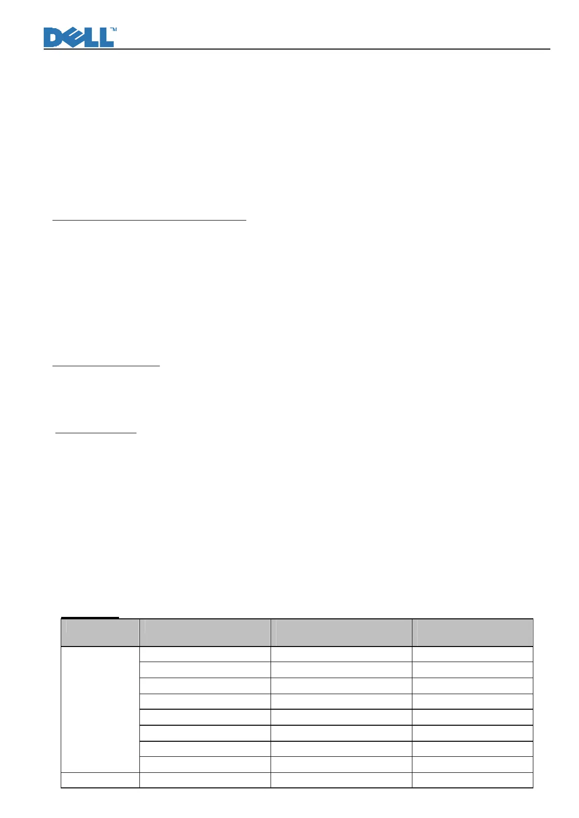
3. FACTORY PRESET TIMING TABLE
3.1 Analog
Standard Resolution Horizontal Frequency
(KHz)
Vertical Frequency
(Hz)
640 x 480 31.469 59.940
640 x 480 37.500 75.000
800 x 600 37.879 60.317
800 x 600 46.875 75.000
1024 x 768 48.363 60.004
1024 x 768 60.023 75.029
1280x1024 48.483 60.042
VESA
1280x1024 60.087 75.034
IBM DOS 720 x 400 31.469 70.087