24
24
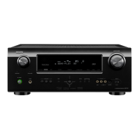
AVR-3805 / AVC-3890
Pin Pin Name Symbol I/O Type Det
Op
(Int.)
Op
(Ext.) Res Function
29 P67/TXD1 TxD/(E2PROM DI) O C - - Ed Z Data transfer output to outside /(E2PROM control pin)
30 P66/RXD1 RxD/(E2PROM DO) I - Lv - Ed Z Data receive input from outside /(E2PROM control pin)
31 P65/CLK1 (E2PROM CLK) O C - - - Z (E2PROM control pin)
32 P64/CTS1 REQ O C - - Ed Z
a
n
u
-
μ
com comm. con
ro
ou
pu
(RTS from sub-
μ
com L)
33 P63/TXD0 MISO O C - - Ed Z Main/Sub-
μ
com comm. control terminal (Data output)
34 P62/RXD0 MOSI I - - - Ed Z Main/Sub-
μ
com comm. control terminal (Data intput)
35 P61/CLK0 DIR CLK O C - - - Z DIR control pin (LC89057W-E), contror clock output
36 P60/CTS0 DIR DIN O C - - Eu Z DIR control pin (LC89057W-E), contror data output
37 P57 DIR DOUT I - - - Eu Z DIR control input pin (LC89057W-E), contror data intput
38 P56 (E2PROM CE) O C - - - Z (E2PROM control pin)
39 P55/EPM (FRASH EPM)/(DL ID) I - Lv - - Z
(Rewrite boot start: L)/(Writing DLINK ID: L,
Writing DSP: H)
40 P54 X'TALRST O C - - - H(Iu) Clock for DIR (L: Osc. Stop)
41 P53 DIR CE O C - - - H(Iu) DIR control pin (LC89057W-E), chip enable output
42 P52 DIR_RST O C - - Ed H(Iu) DIR control output (LC89057W-E) Reset: L
43 P51 SELCLK2 O C - - - Z
ADC/DIR data,clock switching control terminal
(ADC, PCM
・
DD
・
DTS: L) (PCM 1/4 sampling
・
DSD: H)
44 P50/CE FRASH CE I - - - - Z Rewrite boot program start: H input set)
45 P47 nPCMDSD O C - - - Z PCM/DSD switching control pin (PCM: L, DSD: H)
46 P46 fsMODE1 O C - - - Z
SBCK/SLRCK dividing set
(No dividing: L, 1/2 divider enable: H)
47 P45 fsMODE0 O C - - - Z
Select operation clock source of DSP output and D/A
(SBCK/SLRCK: L, RMCK divided: H (only 64fs/fs))
(Fixed to L)
48 P44 MCKf O C - - - Z Not used (Fixed to L)
49 P43 DLINK ON O C - - - Z DENON LINK ON terminal (DENON LINK: H)
50 P42 INT2 I - - - Eu Z DIR2 control pin (LC89057W-E)
51 P41 INT3 I - - - Eu Z DIR3 control pin (LC89057W-E)
52 P40 RSV2 O C - - - Z Not used (Fixed to L)
53 P37 DINA O C - - - Z Digital input switching
54 P36 DINB O C - - - Z Digital input switching
55 P35 DINC O C - - - Z Digital input switching
56 P34 DRECA O C - - - Z Digital RECOUT switching
57 P33 DRECB O C - - - Z Digital RECOUT switching
58 P32 DRECC O C - - - Z Digital RECOUT switching
59 P31 RSV1 O C - - - Z Not used (Fixed to L)
60 VCC VCC - - - - - - +5V
61 P30 NC O C - - - Z Not used
62 VSS VSS - - - - - - GND
63 P27 I/O8 I/O C - - - Z DSP comm. Terminal
64 P26 I/O7 I/O C - - - Z DSP comm. Terminal
65 P25 I/O6 I/O C - - - Z DSP comm. Terminal
66 P24 I/O5 I/O C - - - Z DSP comm. Terminal
67 P23 I/O4 I/O C - - - Z DSP comm. Terminal
68 P22 I/O3 I/O C - - - Z DSP comm. Terminal
69 P21 I/O2 I/O C - - - Z DSP comm. Terminal
70 P20 I/O1 I/O C - - - Z DSP comm. Terminal
71 P17/INT5 NC O C - - - Z Not used
72 P16/INT4 NC O C - - - Z Not used
73 P15/INT3 NC O C - - - Z Not used
74 P14/D12 NC I C - - - Z Not used
75 P13/D11 NC I C - - - Z Not used
76 P12/D10 NC O C - - - Z Not used
77 P11/D9 NC O C - - - Z Not used
78 P10/D8 NC O C - - - Z Not used
79 P07/D7 ROM_RST1 O C - - Ed Z Memory reset for DSP (reset: L)
80 P06/D6 DSP1_RS O C - - Ed Z DSP reset output pin (reset: L)
81 P05/D5 DSP I/0 POWER O C - - Eu Z POWER ON="L" (After 10ms from DIGITAL POWER ON)
82 P04/D4 DSP OSC ON O C - - - Z ON="L" (After 20ms from DIGITAL POWER ON)
83 P03/D3 IRQ1_B1 I - - - - Z Fixed to high impedance
84 P02/D2 FLAG 0A I - - - Ed Z E2PROM chip select control for DSP
85 P01/D1 FLAG 1A I - Lv - Eu Z Not used
86 P00/D0 FLAG 2A(BUSY1) I - Lv - Eu Z DSP operation check flag (FLAG 2A) Normal = "L"
87 P107/AN7 FLAG 3A I - Lv - Eu Z Special Flag
for ROM update (ADSP21061L-A: FLAG 3A)
88 P106/AN6 SELCLK1 O C - - - Z
a
a,c
oc
sw
c
ng con
ro
erm
na
(ADC, PCM 1/4 sampling: L) (PCM
・
DD
・
DTS
・
DSD: H)
 Loading...