33
33
AVR-3805 / AVC-3890
L/R-TVR-REF
20kohm
L/R-TVR-IN
L/R-TVR-OUT
L/R-MVR-OUT
50kohm
20kohm
L/R-MVR-AGND
L/R-MVR-IN
Function
Pin
No.
Pin Name I/O
* For latch-up countermeasure, perform each power supply ON/OFF in the same timing.
28 XOUT O X’tal osc. connecting output terminal
29 XIN I X’tal osc. connection, external clock input terminal (24.576MHz or 12.288MHz)
30 DVDD — Digital power
31 DGND — Digital GND
32 EMPHA/UO I/O Emphasis information/U-data output/Chip address setting terminal
33 AUDIO/VO I/O Non-PCM detect/V-flag output/ Chip address setting terminal
34 CKST I/O Clock switch transition period output/Demodulation master or slave function switching terminal
35 INT I/O Interrupt output for µcom (Interrupt factor selectable)/Modulation or general I/O switching terminal
36 RERR O PLL lock error, data error flag output
37 DO O µcom I/F, read out data output terminal (3-state)
38 DI I µcom I/F, write data input terminal
39 CE I µcom I/F, chip enable input terminal
40 CL I µcom I/F, clock input terminal
41 XMODE I System reset input terminal
42 DGND — Digital GND
43 DVDD — Digital power
44 TMCK/PIO0 I/O 256fs system clock input for modulation/General I/O in/output terminal
45 TBCK/PIO1 I/O 64fs bit clock input for modulation/General I/O in/output terminal
46 TLRCK/PIO2 I/O fs clock input for modulation/General I/O in/output terminal
47 TDATA/PIO3 I/O Serial audio data input for modulation/General I/O in/output terminal
48 TXO/PIOEN O/I Modulation data output/ General I/O enable input terminal
28
272
1613
1712
1811
1910
209
218
227
236
245
254
26
VDD
Tr i m V R
0~+24dB/
1dB step
Tr i m V R
0~+24dB/
1dB step
Main VR
0~-95dB/
0.5dB step
Main VR
0~-95dB/
0.5dB step
DATA
STB
CS2
NC
MVR-IN
NC
MVR-A-GND
MVR-OUT
TVR-OUT
TVR-IN
TVR-REF
3
VSS
CK
GND
CS1
NC
MVR-IN
NC
MVR-A-GND
MVR-OUT
TVR-OUT
TVR-IN
TVR-REF
1
NCNC
1514
NCNC
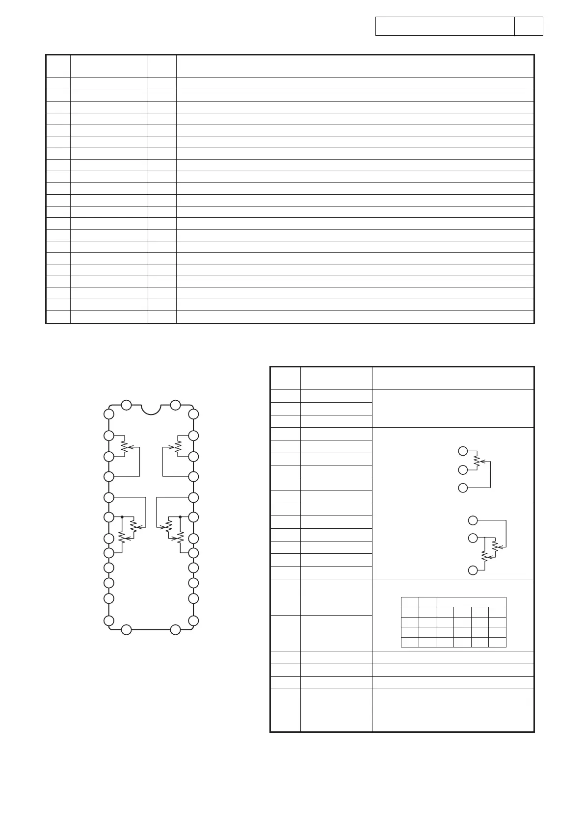
TC94A32FG (AD: IC371, 373, 376, 378)
Function
Pin
No.
Pin Name
2 VSS
27 VDD
12 GND
3 L-TVR-REF Trim volume circuit
26 R-TVR-REF
4 L-TVR-IN
25 R-TVR-IN
5 L-TVR-OUT
24 R-TVR-OUT
6 L-MVR-OUT Main volume circuit
23 R-MVR-OUT
7 L-MVR-AGND
22 R-MVR-AGND
9 L-MVR-IN
20 R-MVR-IN
Chip select code switching input
11 CS1
18 CS2
13 CK Clock input pin for data transfer
16 DATA A-SW control data input pin
17 STB Strobe input pin for data writing
1, 28,
8, 21, NC
10,19,
14,15
CS1 CS2
L L0001
HL1001
L H0101
HH1101
Chip select code
TC94A32FG Terminal Function
 Loading...