NJM2595MTE1 (VIDEO : U5001)
NJM2586AVC3(VIDEO : U5002)
NJM2595
- 1 -
5-INPUT 3-OUTPUT VIDEO SWITCH
■ GENERAL DESCRIPTION ■ PACKAGE OUTLINE
■ FEATURES
● 5-input 3-output
● Operating Voltage ±4.0 to ±6.5V
● Operating current ±15mAtyp. at Vcc=±5V
● Crosstalk -65dBtyp.
● Internal 6dB Amplifier
● Internal 75Ω Driver
● Bipolar Technology
● Package Outline DIP16,DMP16
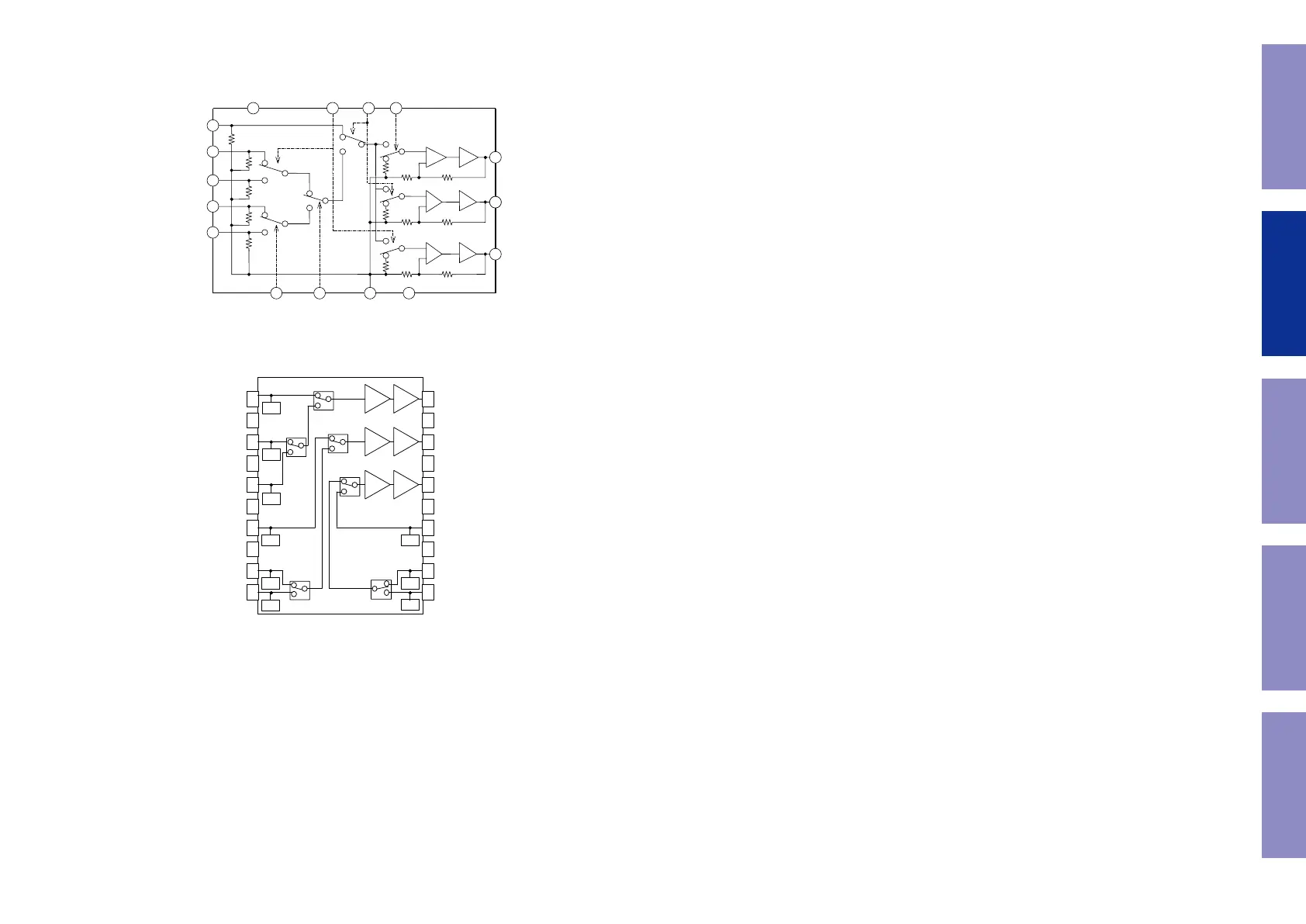
■ PIN CONFIGURATION and BLOCK DIAGRAM
13
9
7
5
3
20k
20k
20k
20k
16
10 14 2
1
15
11
81264
6dB
Amp
75Ω
Driver
S3
S2
S4
S1
20k
20k
20k
S5
S6
S7
Vin1
Vin2
Vin3
Vin4
Vin5
SW3 SW4
SW5SW1SW2V
+
GND V
-
Vout3
Vout2
Vout1
6dB
Amp
6dB
Amp
75
Ω
Driver
75
Ω
Driver
The NJM2595 is a 5-input 3-output video switch. Its switches
select one from five signals received from VTR,TV,DVD,
TV-GAME and others.
The NJM2595 is designed for audio items, such as AV amplifier
and others.
NJM2595D NJM2595M
-
WIDE BAND 3-INPUT 1-OUTPUT 3-CIRCUIT VIDEO AMPLIFIER
QGENERAL DESCRIPTION QPACKAGE OUTLINE
The NJM2586A is a wide band 3-input 1-output 3-circuit video
amplifier. It is suitable for Y, Pb, and Pr signal because frequency
range is 50MHz.The NJM2586A is suitable for AV receiver, STB,
and other high quality AV systems.
Q FEATURES
O Operating Voltage ±4.5 to ±5.5V
O Wide frequency range 0dB at 50MHz typ.
O Internal 3 input-1output 3-circuit video switch
O Internal 6dB Amplifier
O Internal 75Ω Driver Circuit (2-system drive)
O Power Save Circuit
O Bipolar Technology
O Package Outline SDIP22, SSOP20-C3 (under development)
QBLOCK DIAGRAM
NJM2586AVC3 NJM2586AL
SDIP22
9
10
8
5
6
7
4
3
2
1
11 12
13
16
15
14
17
18
19
20
21
22
CH1 IN1
CH1 IN3
CH1 IN2
SW1
SW2
GND
CH1 OU
CH3 IN2
CH3 IN3
V
+
2
CH2 IN3
CH2 IN1
CH3 OU
CH3 IN1
V
+
1
CH2 IN2
V
-
2
PS
75Ω
Driv er
Bias
Cont2
Cont1
Cont1
Cont2
Cont1
Cont2
6dB
mp
Bias
Bias
Bias
Bias
Bias
Bias
Bias
75Ω
Driv er
75Ω
Driv er
Bias
6dB
9
10
8
5
6
7
4
3
2
1
11
14
13
12
15
16
17
18
19
20
CH1 IN1
CH1 IN3
CH1 IN2
SW1
SW2
GND
CH1 OU
V
-
1
CH2 OU
CH3 IN2
CH3 IN3
V
+
2
CH2 IN3
CH2 IN1
CH3 OU
CH3 IN1
V
+
1
CH2 IN2
V
-
2
PS
75Ω
Dr iv er
Bias
Cont2
Cont1
Cont1
Cont2
Cont1
Cont2
6dB
mp
Bias
Bias
Bias
Bias
Bias
Bias
Bias
75Ω
Dr iv er
75Ω
Dr iv er
Bias
6dB
mp
6dB
mp
SSOP20-C3
Before Servicing
This Unit
Electrical Mechanical Repair Information Updating
60
 Loading...