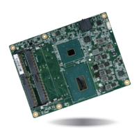
www.dfi .comChapter 3 Hardware Installation
25
Chapter 3
Signal Pin# Pin Type Pwr Rail /Tolerance CH960 PU/PD Module Base Specification R2.1 Description COM Express Carrier Design Guide R2.0 Description
THRM# B35 I CMOS 3.3V / 3.3V PU 10Kɏ
to 3.3V Input from off-Module temp sensor indicating an over-temp situation.
Thermal Alarm active low signal generated by the external
hardware to indicate an over temperature situation. This signal
can be used to initiate thermal throttling.
THRMTRIP# A35 O CMOS 3.3V / 3.3V
PU 10Kɏ to 3.3V
Active low output indicating that the CPU has entered thermal shutdown.
Thermal Trip indicates an overheating condition of the
processor. If 'THRMTRIP#' goes active the system immediately
transitions to the S5 State (Soft Off).
Signal Pin# Pin Type Pwr Rail /Tolerance CH960 PU/PD Module Base Specification R2.1 Description COM Express Carrier Design Guide R2.0 Description
SMB_CK B13 I/O OD CMOS 3.3V Suspend/3.3V
PU 2.2
end
System Management Bus bidirectional clock line. System Management Bus bidirectional clock line
SMB_DAT B14 I/O OD CMOS 3.3V Suspend/3.3V
PU 2.2Kɏ to 3.3V
Sus
end
System Management Bus bidirectional data line. System Management bidirectional data line.
SMB_ALERT# B15 I CMOS 3.3V Suspend/3.3V
PU 2.2Kɏ to 3.3V
Suspend
System Management Bus Alert – active low input can be used to generate
an SMI# (System Management Interrupt) or to wake the system.
System Management Bus Alert
Signal Pin# Pin Type Pwr Rail /Tolerance CH960 PU/PD Module Base Specification R2.1 Description COM Express Carrier Design Guide R2.0 Description
GPO0 A93
GPO1 B54
GPO2 B57
GPO3 B63
GPI0 A54 PU 47Kɏ to 3.3V
GPI1 A63 PU 47Kɏ to 3.3V
GPI2 A67 PU 47Kɏ to 3.3V
GPI3 A85 PU 47Kɏ to 3.3V
Signal Pin# Pin Type Pwr Rail /Tolerance CH960 PU/PD Module Base Specification R2.1 Description COM Express Carrier Design Guide R2.0 Description
VCC_12V
A104~A109
B104~B109
C104~C109
D104~D109
Power
Primary power input: +12V nominal. All available VCC_12V pins on the
connector(s) shall be used.
VCC_5V_SBY B84~B87 Power
Standby power input: +5.0V nominal. If VCC5_SBY is used, all
available VCC_5V_SBY pins on the connector(s) shall be used. Only
used for standby and suspend functions. May be left unconnected if
these functions are not used in the system design.
VCC_RTC A47 Power Real-time clock circuit-power input. Nominally +3.0V.
Thermal Protection Si
General Purpose Outputs for system specific usage.
General Purpose Input for system specific usage. The signals are
pulled up by the Module.
Power and GND Si
I CMOS 3.3V / 3.3V General purpose input pins. Pulled high internally on the Module.
GPIO Si
O CMOS
General purpose output pins. Upon a hardware reset, these outputs should
be low.
3.3V / 3.3V
 Loading...