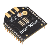
XBee‐PRO®900HP/XBee‐PRO®XSCRFModules
©2014DigiInternationalInc. 24
XBee-PRO 900HP SPI Operation
This section specifies how SPI is implemented on the XBee, what the SPI signals are, and how full duplex
operations work.
XBee Implementation of SPI
The module operates as a SPI slave only. This means that an external master will provide the clock and will
decide when to send. The XBee-PRO 900HP supports an external clock rate of up to 3.5 Mbps.
Data is transmitted and received with most significant bit first using SPI mode 0. This means the CPOL and
CPHA are both 0. Mode 0 was chosen because it's the typical default for most microcontrollers and would
simplify configuration of the master. Further information on Mode 0 is not included in this manual, but is well-
documented on the internet.
XBee-PRO 900HP SPI Signals
The official specification for SPI includes the four signals SPI_MISO, SPI_MOSI, SPI_CLK, and SPI_SSEL.
Using only these four signals, the master cannot know when the slave needs to send and the SPI slave cannot
transmit unless enabled by the master. For this reason, the SPI_ATTN
signal is available in the design. This
allows the module to alert the SPI master that it has data to send. In turn, the SPI master is expected to
assert SPI_SSEL
and start SPI_CLK, unless these signals are already asserted and active respectively. This,
in turn, allows the XBee module to send data to the master.
The table below names the SPI signals and specifies their pinouts. It also describes the operation of each pin:
Note: By default, the inputs have pull-up resistors enabled. See the PR command to disable the pull-up
resistors. When the SPI pins are not connected but the pins are configured for SPI operation, then the pull-ups
are needed for proper UART operation.
Full Duplex Operation
SPI on XBee requires usage of API mode (without escaping) to packetize data. However, by design, SPI is a
full duplex protocol, even when data is only available in one direction. This means that whenever data is
received, it will also transmit, and that data will normally be invalid. Likewise, whenever data is transmitted,
invalid data will probably be received. The means of determining whether or not received data is invalid is by
packetizing the data with API packets.
SPI allows for valid data from the slave to begin before, at the same time, or after valid data begins from the
master. When the master is sending data to the slave and the slave has valid data to send in the middle of
receiving data from the master, this allows a true full duplex operation where data is valid in both directions
for a period of time. Not only must the master and the slave both be able to keep up with the full duplex
operation, but both sides must honor the protocol as specified.
An example follows to more fully illustrate the SPI interface while valid data is being sent in both directions.
Signal Name Pin Number
Applicable AT
Command
Description
SPI_MISO
(Master In, Slave out)
4ATP2
When SPI_SSEL
is asserted (low) and SPI_CLK is active,
the module outputs the data on this line at the SPI_CLK
rate. When SPI_SSEL
is de-asserted (high), this output
should be tri-stated such that another slave device can
drive the line.
SPI_MOSI
(Master out, Slave in)
11 ATD4
The SPI master outputs data on this line at the SPI_CLK
rate after it selects the desired slave. When the module is
configured for SPI operations, this pin is an input.
SPI_SSEL
(Slave Select)
(Master out, Slave in)
17 ATD3
The SPI master outputs a low signal on this line to select
the desired slave. When the module is configured for SPI
operations, this pin is an input.
SPI_CLK
(Clock)
(Master out, Slave in)
18 ATD2
The SPI master outputs a clock on this pin, and the rate
must not exceed the maximum allowed, 3.5 Mbps. When
the module is configured for SPI operations, this pin is an
input.
SPI_ATTN
(Attention)
(Master in, Slave out)
19 ATD1
The module asserts this pin low when it has data to send to
the SPI master. When this pin is configured for SPI
operations, it is an output (not tri-stated).
 Loading...