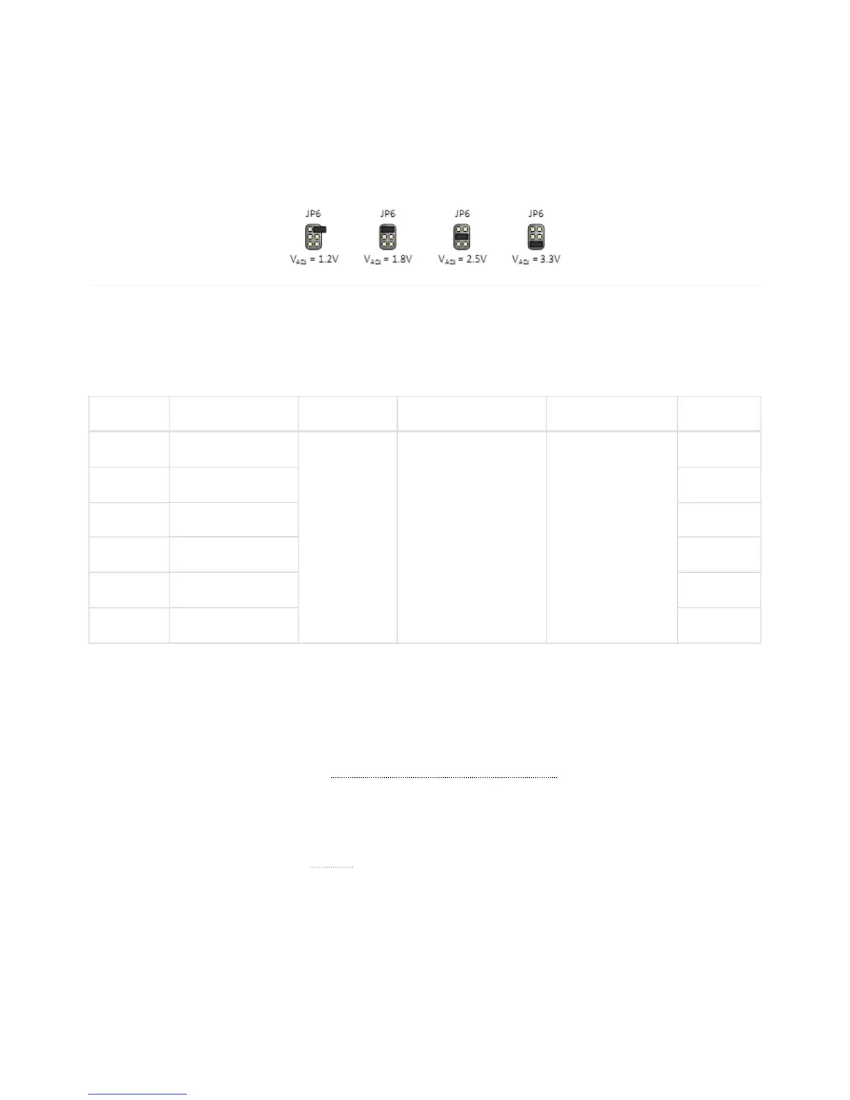
are listed in Figure 2. If JP6 is not set, the VADJ voltage defaults to 1.2 V. This feature enables setting the VADJ voltage to suit
a certain FMC mezzanine card or application. It is recommended to only change the JP6 position with the power switch in the
OFF position.
Please note that for proper voltage levels in digital signals connected to VADJ-powered FPGA banks (ex. user push-buttons),
the correct I/O standard still needs to be set in the design user constraints (XDC or UCF file). See the schematic and/or the
constraints file to determine which signals are in VADJ-powered banks. The provided master UCF and XDC files assume the
default VADJ voltage of 1.2V, declaring LVCMOS12 as the I/O standard for these signals.
I C-interfaced monitoring circuits, INA219 from Texas Instruments, are available on the main power rails. These allow real-
time voltage, current, and power readings in the FPGA. Six such circuits share the same I C bus with different slave addresses.
These are summarized in Table 3, along with recommended configuration values.
Supply rail I2C device address Shunt resistor Configuration register Calibration register Designator
VCC1V0 b1000101 5 mΩ 0x0867 0x4000 IC29
VCC1V5 b1001100 IC33
VCC1V8 b1001000 IC35
VADJ b1000001 IC34
VCC3V3 b1000100 IC44
VCC5V0 b1000000 IC46
Table 3. Power monitoring circuit parameters.
The configuration and calibration registers are volatile, so they need to be initialized after power-up. After initialization is done
voltage, current, and power values can be read from dedicated registers. It is recommended to add glitch filters to the I2C
master controller to avoid spurious start or stop conditions occurring on the bus. This is especially important when using an
external I2C master connected to the J18 header (not mounted by default).
For more information on the INA219, see its
datasheet (http://www.ti.com/lit/gpn/ina219).
The principle of operation is measuring bus and shunt voltages using a programmable-gain differential amplifier and an analog-
to-digital converter. The schematic for one such circuit is shown in Figure 3. The two analog inputs are connected across a
shunt resistor placed in series between the power supply and the load. Current consumed by the load produce a voltage drop
across the shunt resistor. This voltage is measured by the INA219 and is used to calculate the current. In addition, the bus
voltage is measured on V- with respect to
GND () and is the voltage on the respective power rail. The voltage and current
measurements are used to calculate power consumption. If the INA219 is configured, it will correctly calculate all three
parameters. In its default, power-up configuration it provides bus and shunt voltage only, which can be used to calculate
current and power in the FPGA.
3. Power Monitoring
2
2
Page 10 of 3