Pmod
conector Power Analog/Digital Routing
Series
protection Recommended usage
JA, JB 3.3 V Digital-only Differential; Pairs:
1-2,3-4,7-8,9-10
0 ohm >=10MHz; LVDS_25 input
JC, JD 3.3 V Digital-only Single-ended 200 ohm <10
MHz (), LVCMOS33
Table 10. Pmod differences.
JXADC is a dual digital/analog Pmod wired to auxiliary analog FPGA input pins (see description below). JA, JB, JC and JD are
digital-only but routed in a different manner. JC and JD signal traces are routed as single-ended signals with no length matching
or characteristic impedance guarantees. JA and JB connector signals, on the other hand, are routed differentially in pairs at 100
ohm characteristic impedance. Inter-pair matching is +- 20mm. The series resistor on these two Pmods are replaced by 0 ohm
shunts, so care must be exercised not to use voltages higher than 3.3V, or short FPGA-driven pins.
For slow digital signals, below 10
MHz (), all Pmod connectors are equivalent, if VADJ is set to 3.3 V (see the Power Supplies
section). For higher frequencies, the routing and series protection need to be taken into account as well.
Pmod Pinouts
JA1: B13 JB1: G14 JC1: K2 JD1: JXADC1: A13
JA2: F14 JB2: P15 JC2: E7 JD2: JXADC2: A15
JA3: D17 JB3: V11 JC3: J3 JD3: JXADC3: B16
JA4: E17 JB4: V15 JC4: J4 JD4: JXADC4: B18
JA7: G13 JB7: K16 JC7: K1 JD7: JXADC7: A14
JA8: C17 JB8: R16 JC8: E6 JD8: JXADC8: A16
JA9: D18 JB9: T9 JC9: J2 JD9: JXADC9: B17
JA10: E18 JB10: U11 JC10: G6 JD10: JXADC10: A18
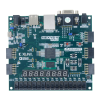
Table 11. Genesys 2 Pmod pin assignments.
Digilent produces a large collection of Pmod accessory boards that can attach to the Pmod expansion connectors to add ready-
made functions like A/D’s, D/A’s, motor drivers, sensors, and other functions. See
Digilent's Pmod category
(http://store.digilentinc.com/pmod-peripheral-modules/) for more information.
The on-board Pmod expansion connector labeled “JXADC” is wired to the auxiliary analog input pins of the FPGA.
Depending on the configuration, this connector can be used to input differential analog signals to the analog-to-digital
converter inside the Kintex-7 (XADC). Any or all pairs in the connector can be configured either as analog input or digital
input-output.
The Dual Analog/Digital Pmod on the Genesys 2 differs from the rest in the routing of its traces. The eight data signals are
grouped into four pairs, with the pairs routed closely coupled for better analog noise immunity. Furthermore, each pair has a
partially loaded anti-alias filter (100 ohm, 1 nF) laid out on the PCB. The filter does not have capacitors C151, C152, C153, and
C154. In designs where such filters are desired, the capacitors can be manually loaded by the user.
NOTE: The coupled routing and the anti-alias filters might limit the data speeds when used for digital signals.
14.1 Dual Analog/Digital Pmod
Page 2
of 3