EasyManua.ls Logo

Dragino LSN50 - Pin Definitions

Dragino LSN50
60 pages
To Next Page IconTo Next Page
To Previous Page IconTo Previous Page
Loading...
www.dragino.com
LSN50 LoRa Sensor Node User Manual 7 / 60
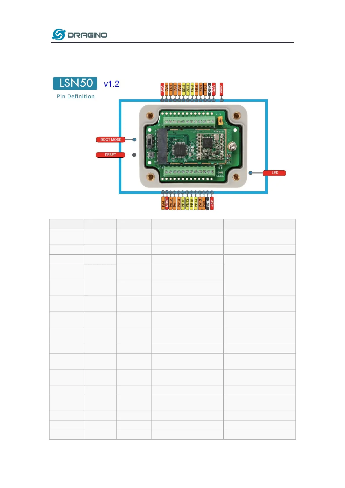
1.5 Pin Definitions
Pin No.
Signal
Direction
Function
Remark
1
VCC(2.9V)
OUTPUT
VCC
Directly connect to main
power for board
2
PA0
In/Out
Directly from STM32 chip
Used as ADC in LSN50 image
3
PA1
In/Out
Directly from STM32 chip
4
PA2
In/Out
Directly from STM32 chip, 10k
pull up to VCC
Used as UART_TXD in LSN50
image
5
PA3
In/Out
Directly from STM32 chip, 10k
pull up to VCC
Used as UART_RXD in LSN50
image
6
PB6
In/Out
Directly from STM32 chip, 10k
pull up to VCC
7
PB7
In/Out
Directly from STM32 chip, 10k
pull up to VCC
8
PB3
In/Out
Directly from STM32 chip, 10k
pull up to VCC
9
PB4
In/Out
Directly from STM32 chip
10
PA9
In/Out
Directly from STM32 chip, 10k
pull up to VCC
11
PA10
In/Out
Directly from STM32 chip, 10k
pull up to VCC
12
GND
Ground
13
VCC(2.9V)
OUTPUT
VCC
Directly connect to main
power for board
14
Jumper
Power on/off jumper
15
PA4
In/Out
Directly from STM32 chip
16
NRST
In
Reset MCU

Related product manuals