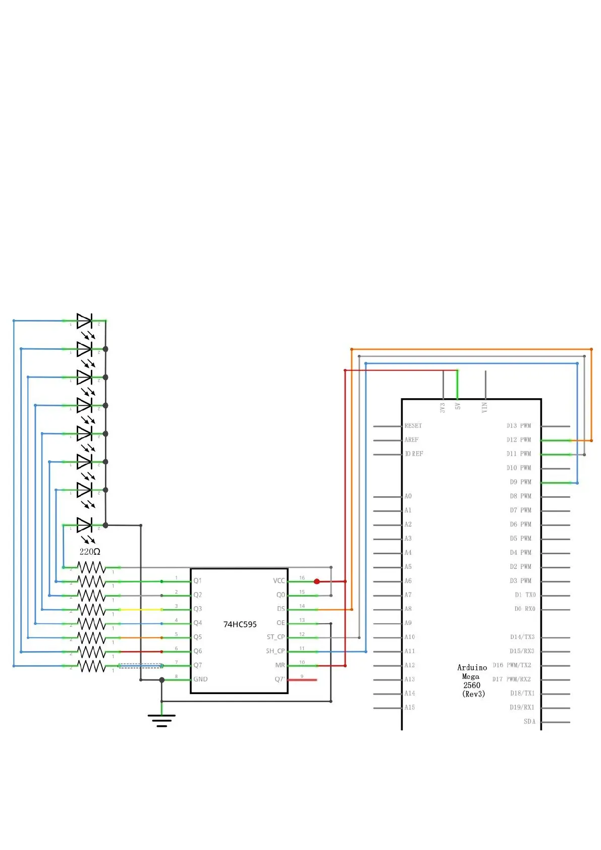
The clock pin needs to receive eight pulses. At each pulse, if the data pin is high,
then a 1 gets pushed into the shift register; otherwise, a 0. When all eight pulses
have been received, enabling the 'Latch' pin copies those eight values to the latch
register. This is necessary; otherwise, the wrong LEDs would flicker as the data is
being loaded into the shift register.
The chip also has an output enable (OE) pin, which is used to enable or disable the
outputs all at once. You could attach this to a PWM-capable MEGA2560 pin and use
'analogWrite' to control the brightness of the LEDs. This pin is active low, so we tie
it to GND.
Connection
Schematic