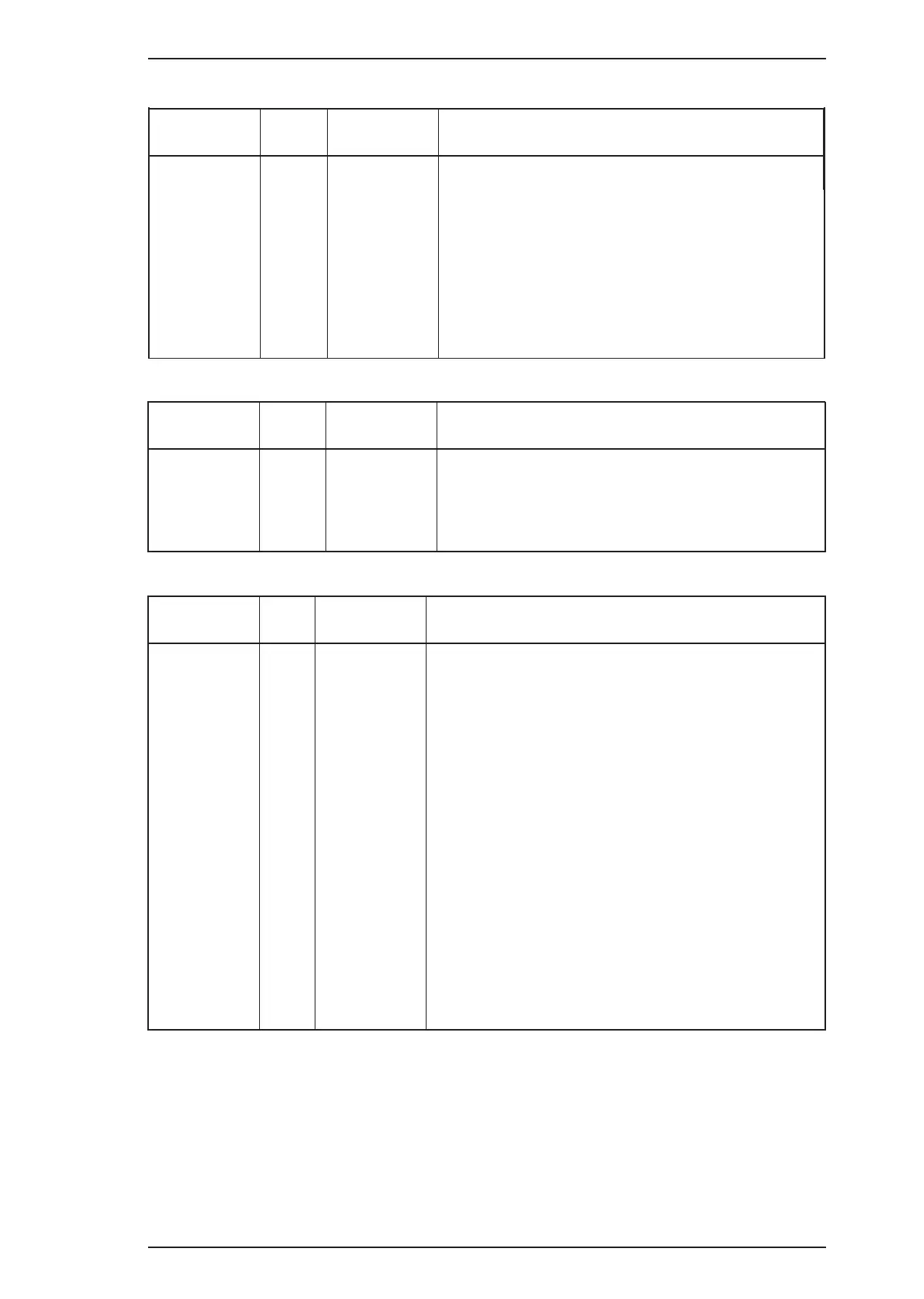
Table A-3. Connector Pin Assignments — CN2
Pin I/O Name Description
1 I DTR
Data terminal ready signal
2 O TXD-
Transmit data signal
3 — GND
Signal Ground
4 I RXD-
Receive data signal
5 O TXD+
Transmit data signal
6 I RXD+
Receive data signal
Table A-4. Connector Pin Assignments — CN3
Pin I/O Name Description
1 O CR-A Carriage motor drive phase A
2 O CR-/A Carriage motor drive phase /A
3 O CR-B Carriage motor drive phase B
4 O CR-/B Carriage motor drive phase /B
Table A-5. Connector Pin Assignments — CN4
Pin I/O Name Description
1 — FG Frame ground
2 — VDD +5VDC
3 I CO Cartridge In/Out sensor
4.6.8 — GND Ground
5 O HCLK Head clock signal
7 O LATCH Head latch signal
9 O SI Serial data signal
10 I ID4 Head ID signal
11.12 — GND2 Ground (for head control voltage)
13.14 O COM Head voltage
15 I ID1 Head ID signal
16 I ID2 ID code (Vh level auto-selection)
17 I ID3 ID code (Vh level auto-selection)
18 I TH Thermister alalog data
19 I M/C Black or Color detection sensor
Epson Stylus Color 200/Epson Stylus 200 Appendix
Rev. A A-3