Page-3
D0-D3 11-14 14,15,16,19 Bi-
(Data bus) direction
A0-A3 4-7 5,7,9,10 Input
(Address bus)
ALE 3 4 Input
(Address Latch Enable)
WR 10 13 Input
(WRite)
RD 8 11 Input
(ReaD)
CS1, CS0 15,2 20,2 Input
(Chip Select)
STD.P 1 1 Output
(STanDard Pulse)
VDD 18 24
GND 9 12
(VDD) 16,17 22,23
N.C. - 3,6,8,17,18,21
Connect these pins to a bidirectional data bus or CPU data bus. Use
this bus to read to and write from the internal counter and registers.
Address input pins used for connection to CPU addresses, etc. Used
to select the RTC's internal counter and registers (address selection).
When the RTC is connected to a multiplexed-bus type of CPU, these
pins can also be used in combination with the ALE described below.
Reads in address data and CS0 state for internal latching.
When the ALE is high, the address data and CS0 state is read into
the RTC. When the (through-mode) ALE falls, the address data and
CS0 state at that point are held. The held address data and CS0 status
are maintained while the ALE is low.
If the RTC is connected to a CPU that does not have an ALE pin and
thus there is no need to use this ALE pin, fix it to VDD.
Writes the data on D0 to D3 into the register of the address specified
by A0 to A3, at the leading edge of WR.
Make sure that RD and WR are never low at the same time.
Outputs data to D0 to D3 from the register at the address specified by
A0 to A3, while RD is low.
Make sure that RD and WR are never low at the same time.
When CS1 is high and CS0 is low, the RTC's chip-select function is
valid and read and write are enabled.
When the RTC is connected to a multiplexed-bus type of CPU, CS0
requires the operation of the ALE (see the description of the ALE).
Use CS1 connected to a power voltage detection circuit. When CS1 is
high, the RTC is enabled; when it is low, the RTC is on standby.
When CS1 goes low, the HOLD and RESET bits in the RTC registers
are cleared to 0.
This is an N-channel open drain output pin.
Depending on the setting of the CE register, a fixed-period interrupt
signal and a pulse signal are output.
The output from this pin cannot be inhibited by the CS
1
and
CS0
signals.
Use a load voltage that is less than or equal to VDD. If not using this
pin, keep it open-circuit.
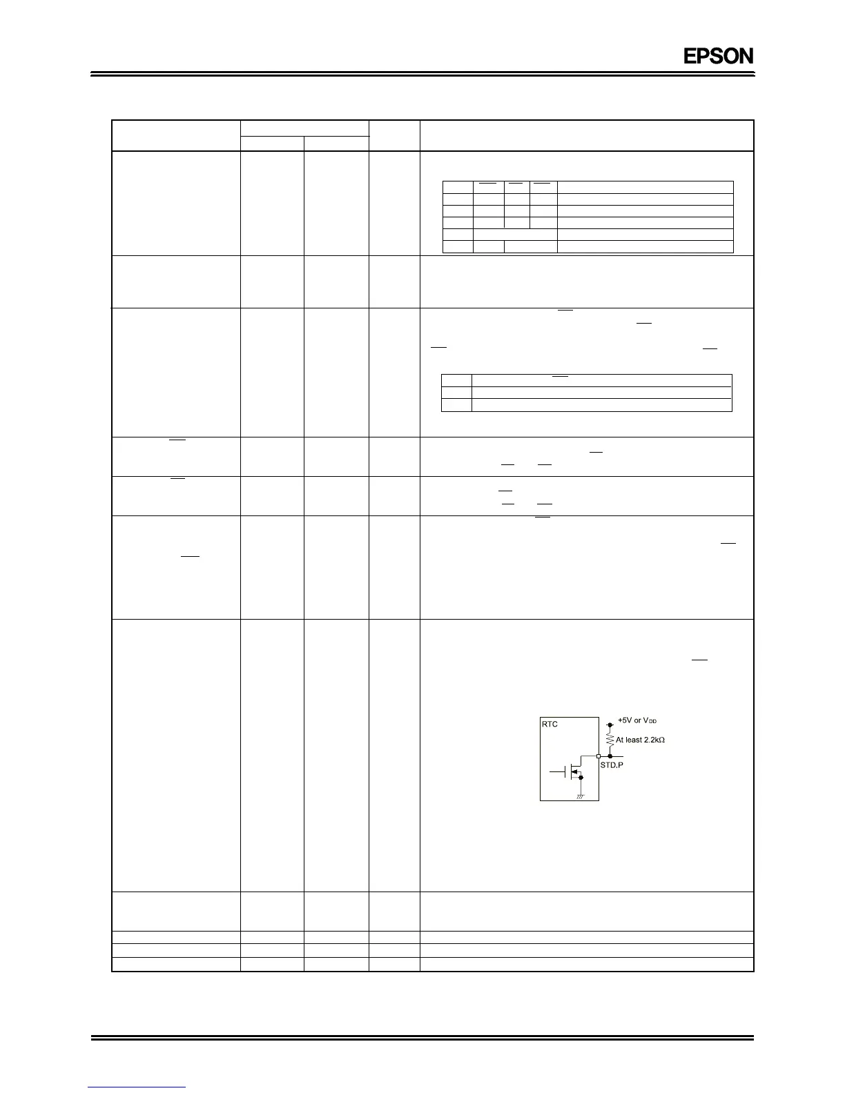
An example of STD.P connection is shown below.
If the STD.P output is not be used during standby operation,
connecting the pull-up resistor to +5 V provides a reduction in current
consumption. If the STD.P output is to be used even during standby,
connect the pull-up resistor to the RTC's VDD. In this case, the current
consumption will be increased by the amount of current flowing
through the pull-up resistor.
Connect this pin to power source. Supply to 5 V ±10% to this pin
during normal operation; at least 2 V during battery back-up
operation.
Connect this pin to ground.
These pins are connected internally to VDD. Leave them open circuit.
These pins are not connected internally. Ground them.
■ Pin functions
Signal Pin No. Input/ Function
RTC-72421RTC-72423 Output
CS-1 CS0 RD WR Mode of D0 to D3
H L L H Output mode (read mode)
H L H L Input mode (write mode)
H L L L Do not use
L H or L High impedance (back-up mode)
H H H or L High impedance (RTC not selected)
ALE Address data and CS0 status
H Read into the RTC to set address data
L Held in the RTC (latched at the trailing edge of the ALE)