2. Schematic Checklist and PCB Layout Design
• Pins SENSOR_VP or SENSOR_VN is recommended for use as ADC.
• If SENSOR_VP and SENSOR_VN are used as GPIOs, while ADC is supported by other pins in the circuit
design, users need to do settings in software to avoid the input glitch.
2.1.7 External Capacitor
Figure 9 shows the schematic of components connected to pin47 CAP2 and pin48 CAP1. C5 (10 nF) that connects
to CAP1 should be of 10% tolerance and is required for proper operation of ESP32. RC circuit between CAP1
and CAP2 pins may be omitted under certain conditions. This circuit is used when entering Deep-sleep mode.
During this process, to minimize power consumption, the voltage to power ESP32 internals is dropped from 1.1
V to around 0.7 V. The RC circuit is used to minimize the period of the voltage drop. If removed, this process will
take longer and the power consumption in Deep-sleep will be higher. If particular application of ESP32 is not using
Deep-sleep mode, or power consumption is less critical, then this circuit is not required.
GND
GND
C5
10nF/6.3V(10%)
GND
49
CAP2
47
CAP1
48
VDDA
46
C6
3.3nF/6.3V(10%)
R1 20K(5%)
Figure 9: ESP32 External Capacitor
2.1.8 UART
Users need to connect a 499 Ω resistor to the U0TXD line in order to suppress the 80 MHz harmonics.
U0TXD
U0RXD
GPIO22
R3 499R
U0TXD
41
GPIO22
39
GPIO21
U0RXD
40
Figure 10: ESP32 UART
2.2 PCB Layout Design
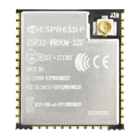
This chapter introduces the key points of designing ESP32 PCB layout with the example of ESP32-WROOM-
32D.
Espressif Systems 8 ESP32 Hardware Design Guidelines V2.7

 Loading...