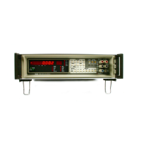
8502A
3-13. The software program consists of two
parailei
processes.
A
background process (Figure
3-3)
is responsible
for interrupt driven activities
such as updating
the display
digits and directing the A/D converter in taking a
sample.
The foreground
process (Figure
3-4)
is responsible for the
measurement
cycle including
accumulating data
from the
background
process
ami
performing
required calculations.
MARK
INTERRUPT
Figure
3-3.
Background Software
Process
3-14. The controller is
structured
around
the Intel 8080
microprocessor.
Figure
3-5
is a
block diagram
of
the
con-
troller
module. Hardware control
functions have been
minimized
by
careful software design.
Sequences of events
are timed
from two sources. Basic
operations of the micro-
processor are run from a 1
.7 MHz clock.
The other source
is generated by
shaped line frequency pulses, which are
applied to a
phase-locked
loop.
The phase-locked loop
multiplies the line
frequency by eight. This signal is used to
generate mark
interrupts which time the background
process.
3-15.
Software for
the
8502A
is stored in five ROM’s.
These
read only memories are mounted on a
“piggy-back”
board, which is
connected to the main controller peb
at
the socket for U25.
Four
RAMs (random
access memory)
are
used for temporary storage of data by the
micropro-
cessor.
Data lines (DB0-DB7) are used for
bidirectional
data
flow. Address lines (AO—
A15)
determine
the source
or
storage
location of data. Since other modules of the 8502A
system are
addressed as memory locations, address and data
I/O controls are used for
access
to
the external bus
structure.
3-16. Interrupts are used to divert the
microprocessor
from the
main program
to service other routines.
Inter-
rupts are
synchronized to an appropriate
lime
in
the
microprocessor cycle through interrupt
control, where
assigned
priorities vector module identity data onto
the
data- bus. Module identity
data
words direct the micro-
processor to the memory location containing the next
instruction. Two interrupts are internally
generated:
ACK
INT
and
MARK INT (priorities one and six
respectively).
ACK INT is
generated when an acknowledge signal is
not
returned, MARK INT is
used to synchronize A/D samples
and display digit updates to
the line frequency.
3-17.
An interrupt may be externally requested by pull-
ing the INT line low.
When
the
microprocessor
is ready to
accept the interrupt, the
interrupt
acknowledge (!NA)
signal is
generated. The requesting module must respond
with
an
ACK and a data bit (on IDl— ID4) which is used
as a priority
vector
by
INT CONTROL.
3-18. Two types of resets may occur:
software
and
hardware.
Software resets are a result of front panel or
remote
requests.
Hardware
resets occur at
power
up
or
power down. Line frequency pulses from RTS are sensed
by the reset logic. At
power
up
the reset signal
assures
that
the microprocessor will start from program location zero.
At
power down the reset signal assures that the controller
will not call up
wrong modules.
3-19,
The
microprocessor
control logic is responsible
for latchirtg up a status
word
at the beginning
of each
instruction cycle and
for telling the microprocessor when
t(.) enter and exit
wait
states. Microprocessor
sequences are
divided
into
machine
states (one clock period,
588 nsec),
machine cycles (from three to
five
states) and instruction
cycles (from one to five machine cycles). Status words
are
used to control and synchronize data I/O, memory read/
write,
and
some of the interrupt control signals. The micro-
processor must be
instructed
to
enter
a
wait state after
addressing an external module and after being
interrupted
to allow
the external module time to respond.
3-3