Main
Board
Input
Amplifier A
input amplifiers A and B are two
matched 300
MHz
ampli-
fier circuits: Channei A and channel B.
Channels A and B are identical except the 100-kHz filter in
channel A,
the switching
circuitry for the
separate/common
modes, the B-channel delay line, and event delay output.
The following description refers to channel A but is also va-
lid for channel B, (see
Figure 4-4).
Four main stages makes the
input
amplifier:
Input stage,
impedance converter stage, comparator stage and buffer
stage.
•
Input Stage
The input stage contains:
-
50 ^2/1 Mf2 impedance selector
-
1X/1 OX attenuator
-
AC/DC coupling
-
Voltage
limiter
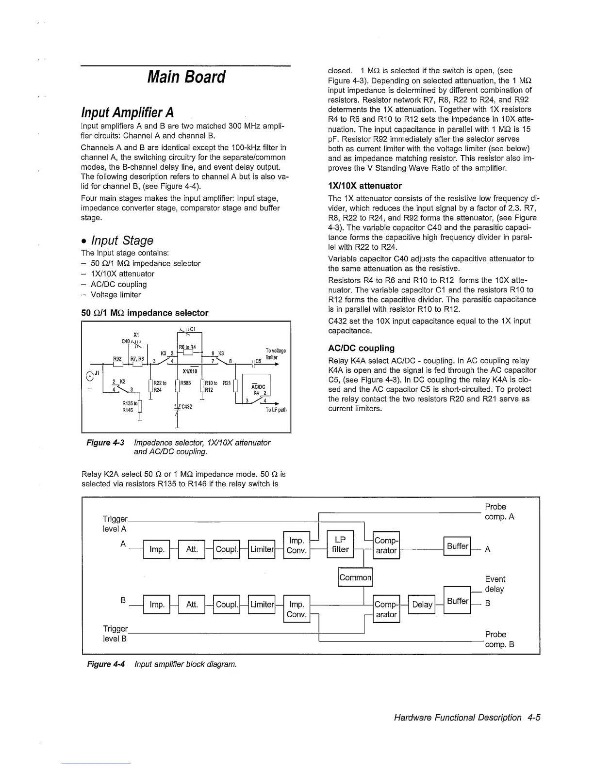
50
Q/1 MQ impedance selector
Figure
4~3
Impedance selector, 1X/1 OX attenuator
and
AC/DC
coupling.
Relay K2A select 50 O or 1 M£2 impedance mode. 50 ^2 is
selected via resistors R135 to R146 if the relay switch is
closed. 1 UQ. is selected if the switch
is
open,
(see
Figure
4-3).
Depending
on
selected attenuation, the 1 MQ
input impedance is determined by
different combination of
resistors. Resistor network R7, R8, R22
to R24, and R92
determents the 1X attenuation.
Together
with
1X
resistors
R4 to
R6
and R10 to R12 sets the impedance in
10X atte-
nuation. The input capacitance in
parallel with
1 M^2
is 15
pF.
Resistor
R92
immediately
after the selector
serves
both
as current limiter with the
voltage
limiter (see below)
and
as impedance
matching resistor.
This resistor also im-
proves the V Standing Wave Ratio of
the amplifier.
1X/10X attenuator
The
IX
attenuator consists
of
the resistive low frequency
di-
vider,
which reduces the input signal
by a factor of 2.3. R7,
R8, R22 to R24, and R92 forms the
attenuator, (see
Figure
4-3).
The variable capacitor C40
and the parasitic
capaci-
tance forms the capacitive high
frequency
divider in paral-
lel with
R22
to
R24.
Variable capacitor
C40
adjusts
the capacitive attenuator
to
the same attenuation as the
resistive.
Resistors R4 to R6 and RIO to R12
forms
the 10X atte-
nuator. The variable capacitor Cl and the
resistors
R10 to
R12 forms the capacitive divider. The parasitic
capacitance
is in parallel with resistor RIO
to
R12.
C432 set the 10X input capacitance equal
to the
IX input
capacitance.
AC/DC coupling
Relay K4A select
AC/DC
-
coupling.
In AC coupling relay
K4A
is open
and the
signal
is
fed through the AC
capacitor
C5, (see Figure
4-3).
In DC coupling
the relay K4A is clo-
sed
and
the
AC
capacitor
C5
is
short-circuited. To
protect
the relay contact the two resistors R20 and R21
serve
as
current limiters.
Probe
B
Trigger
level B
Imp.
—
Att.
—
Coupl.
—
Limiter
—
Imp.
Conv.
Common
Comp“|
arator
Delay
^
—
Buffer!
Event
,
delay
B
Probe
comp.
B
Figure
4-4
input amplifier block diagram.
Hardware
Functional
Description
4-5
 Loading...