Voltage
limiter
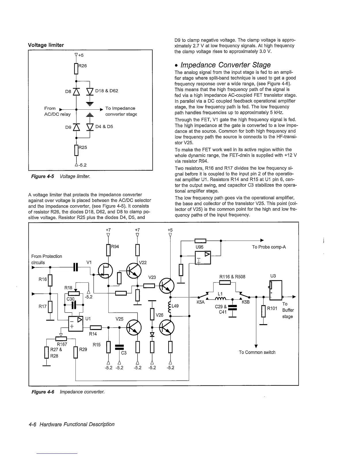
Figure
4~5
Voltage limiter.
A
voltage limiter that protects the
impedance converter
against over voltage is
placed between the AC/DC selector
and the impedance
converter, (see Figure
4-5).
It
consists
of resistor R26,
the diodes D18, D62, and
D8 to clamp po-
sitive
voltage. Resistor R25 plus
the
diodes D4, D5, and
D9
to
clamp
negative voltage. The clamp voltage is
appro-
ximately
2.7
V
at
low frequency signals. At high
frequency
the
clamp
voltage
rises to approximately 3.0 V.
•
Impedance
Converter
Stage
The analog
signal from the
input
stage
is fed
to
an
ampli-
fier
stage
where split-band
technique is used to get a good
frequency
response over a wide range, (see Figure
4-6).
This
means that
the
high frequency path of the signal is
fed via a
high impedance
AC-coupled
FET
transistor
stage.
In
parallel via a
DC coupled feedback operational amplifier
stage, the
low frequency
path
is
fed. The low frequency
path
handles
frequencies
up to approximately 5 kHz.
Through
the
FET, V1 gate the high
frequency signal is fed.
The
high
impedance
at the gate is converted to a low
impe-
dance
at the source.
Common
for both high frequency and
low
frequency path
the source is connects to the
HF-transi-
stor
V25.
To make
the
FET work well in
its active
region
within the
whole
dynamic
range, the
FET-drain
is
supplied with
+12
V
via resistor R94.
Two
resistors, R16 and R17
divides the low frequency si-
gnal
before
it is coupled
to
the input pin 2 of the operatio-
nal
amplifier U1.
Resistors R14 and R15 at U1 pin
6,
cen-
ter the
output
swing, and
capacitor
C3
stabilizes
the opera-
tional
amplifier stage.
The
iow
frequency
path goes via the operational amplifier,
the
base and
collector of the transistor V25. This point
(col-
lector of V25)
is the common point for the high and
low fre-
quency
paths of the input
frequency.
Figure
4-6
Impedance converter.
4-6
Hardware
Functional
Description