A
driver stage
(V22), an output stage (V23), and a current
generator
(V26),
forms an amplifier with
high
output cur-
rent.
This
amplifier
is used to get a linear output in the
100Q load resistor R101
over
a
swing of
2 V.
From the output
of this
second amplifier
stage, the signal
goes back to
the
operational amplifier pin 3 via divider R27
to R29 and R167. Trim potentiometer R167 sets the gain
of
the
low
frequency path equal to the high frequency gain,
(about
0.9).
Capacitor C30 is connected to U1 pin 1 and 8
to
achieve
stable
operation. The trim
potentiometer
R18
be-
tween pin 1 and 5 on U1 is used to adjust the offset volt-
age of the operational
amplifier.
The channel A filter connected to the output of the second
amplifier stage is a
100 kHz LC-fiiter. It consists
of
coil LI,
and
two
capacitors,
C29 and C41 in paraiiei. Two reiay-
contacts, K5A and K5B, controis the filter. The filter output
is connected to
the
input of
the
comparator stage.
The output of the ampiifier stage is aiso connected to the
rear panel via the ampiifier U95. By using this output cailed
"PROBE
COMPENSATiON A" it is possibie to compensate
a probe connected to the counter. This voitage is aiso con-
nected to
an analog input in the p-controiier. This makes it
possibie for the
p-controiler
to get a quick
knowledge
about
the input voltage.
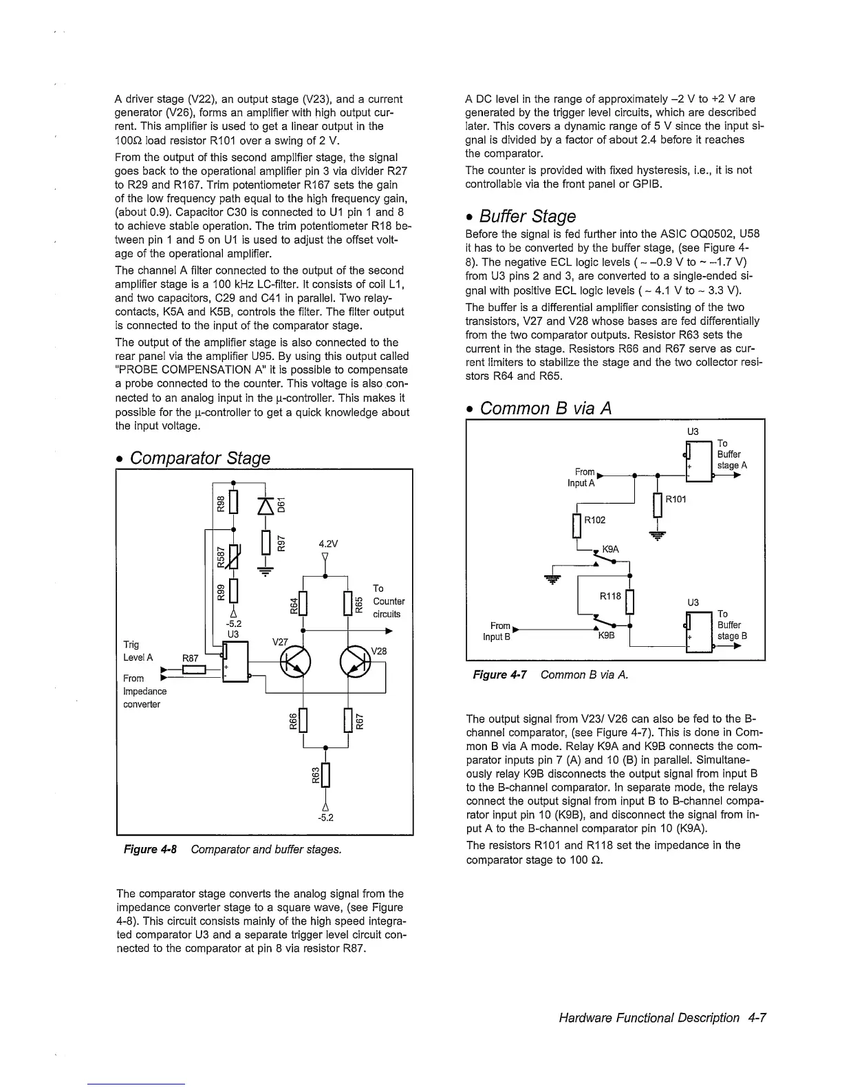
Figure
4-8
Comparator
and
buffer
stages.
A DC level in the range of
approximateiy
-2
V to
+2
V
are
generated by the trigger
level circuits,
which are
described
later.
This
covers
a
dynamic range
of 5 V since the
input
si-
gnal is
divided
by a
factor
of
about 2.4 before it
reaches
the comparator.
The counter is provided with fixed
hysteresis,
i.e.,
it is not
controllable via the front panei or GPiB.
•
Buffer
Stage
Before the
signal is fed
further into
the ASiC OQ0502,
U58
it has to be converted by the buffer stage, (see
Figure
4-
8).
The negative
ECL
logic
levels
(
~
-0.9
V to
—
1.7
V)
from U3 pins 2 and
3,
are converted to
a
single-ended
si-
gnal with positive ECL logic levels
(
~
4.1
V
to
~
3.3 V).
The buffer is a differentiai ampiifier consisting of the
two
transistors, V27 and V28 whose
bases
are fed different! aliy
from the two comparator outputs. Resistor R63
sets
the
current in
the stage.
Resistors
R66 and R67 serve as
cur-
rent limiters to stabiiize the stage and the two
collector
resi-
stors
R64
and
R65.
•
Common
B via A
Figure
4-7
Common B via A.
The output signa! from
V23/ V26
can also
be
fed to the B-
channel comparator, (see Figure
4-7).
This
is
done in Com-
mon B via A mode. Reiay K9A and K9B
connects the
com-
parator inputs pin
7
(A) and
10
(B) in paraiiei. Simultane-
ously relay
K9B disconnects the
output signal from input
B
to the B-channel comparator, in separate
mode, the relays
connect the output signal from
input
B
to
B-channel compa-
rator input pin
10
(K9B), and disconnect the
signal
from
in-
put A to the B-channel comparator pin
10
(K9A).
The resistors R101 and R118
set the
impedance in the
comparator
stage
to
100 Q.
The
comparator
stage converts
the anaiog signa! from
the
impedance
converter
stage to a square
wave,
(see Figure
4-8).
This
circuit
consists mainly of the high speed integra-
ted comparator
U3 and a separate trigger
ievel
circuit con-
nected
to the
comparator
at pin 8 via resistor R87.
Hardware Functional
Description
4-7
 Loading...