Power
Supply
•
Primary
Circuits
The
power
supply generates five regulated
DC supply volta-
ges to the
counter. It also generates some
other supply vol-
tages
for
special
purposes. The
power
supply block also
contains
the ON/STANDBY logic, (see Figure
4-12).
The main
building-block
of
the
power supply is the
primary
switch
mode power circuits. A rectifier make
a DC-voltage
of
the line power
AC-voltage
(90
V to 265 V), before
it is
fed
to
the switch
circuits.
After a line-power
filter
in
the power inlet, a fuse and
an
NTC-resistor
protect the power supply. The
fuse
(FI)
should only blow
if
a catastrophic error occurs on
the
pri-
mary side
of the power supply, A
short-circuit
on the secon-
dary side should not affect the primary side.
To
minimize
the "current rush" to the capacitors at the
connection
of the
power cord, an NTC-resistor (R337) is used.
The resistan-
ce is
16^2
when
the resistor is
cold,
but decrease to a few
ohms when warmed up by the current.
The
AC voltage is
rectified in the bridge rectifier D40 and
filtered
in C330.
Cl
81,
Cl
83,
and
Cl
84
should suppress noise from
D40.
L20, Cl
73,
and C174 forms filters.
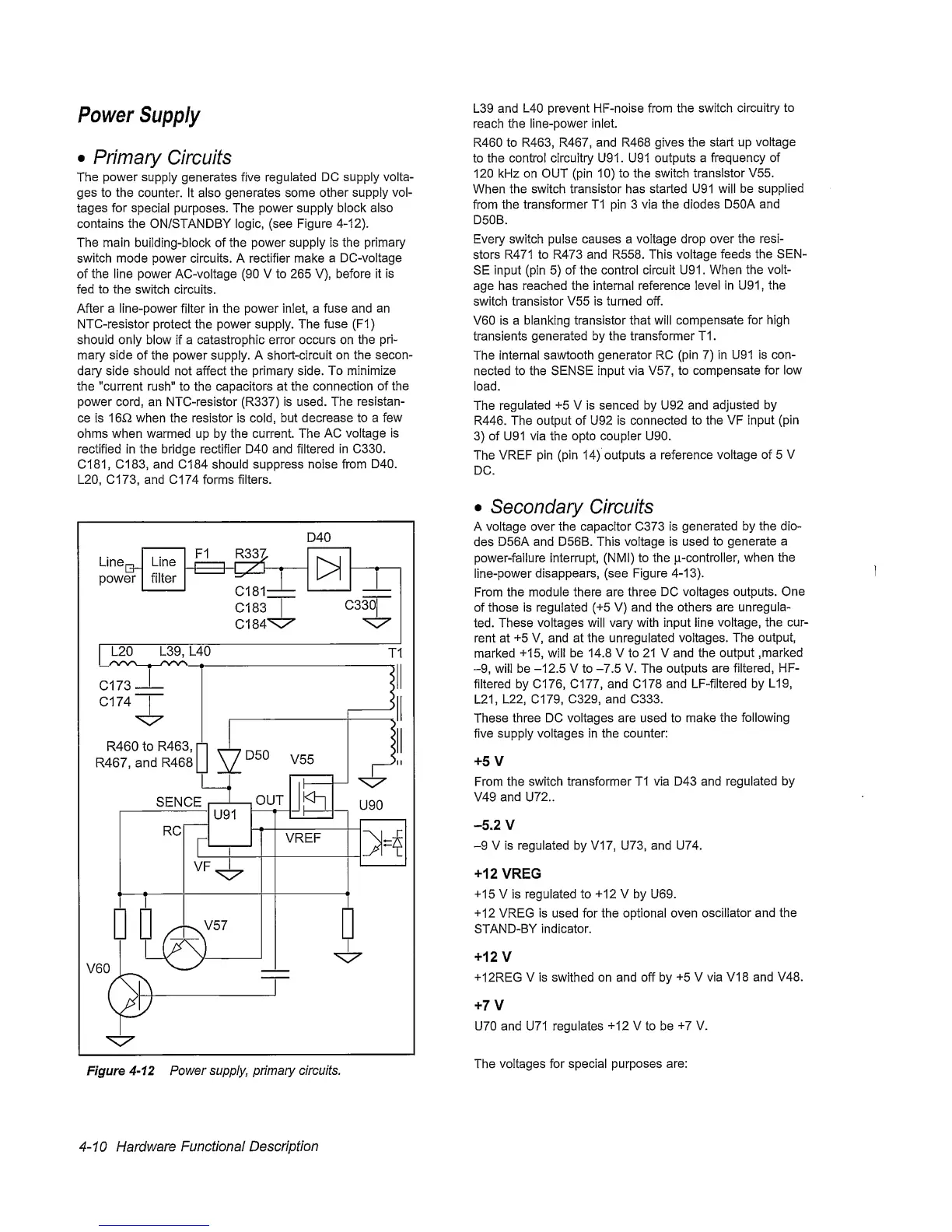
D40
Uneg_
power
Line
F1
R33Z
w
filter
I
1
I
C181—
L-
C183
0184^^
C330|
L20 L39, L40
T1
Cl
73.
C174'
R460 to R463,
R467,
and
R468
SENCE
RC
V60
I
D50
V55
OUT
U91
VF
V57
VREF
U90
3
=
Figure
4-12
Power supply, primary circuits.
L39 and L40
prevent HF-noise from
the switch
circuitry
to
reach the
line-power inlet.
R460 to R463, R467,
and
R468
gives the start up
voltage
to the control
circuitry
U91. U91
outputs a frequency of
120 kHz on OUT (pin
10)
to the
switch
transistor V55.
When the switch transistor has started U91
will
be
supplied
from the
transformer T1
pin
3 via the diodes
D50A
and
D50B.
Every
switch pulse causes a voltage drop
over
the resi-
stors
R471
to R473 and R558. This
voltage
feeds the
SEN-
SE input (pin
5)
of
the control
circuit U91. When
the volt-
age has reached the internal reference
level in U91, the
switch
transistor
V55
is turned
off.
V60 is a blanking transistor that will
compensate for high
transients generated
by
the transformer T1.
The
internal
sawtooth generator RC (pin
7)
in
U91 is con-
nected to the
SENSE input via
V57, to
compensate
for low
load.
The
regulated
+5
V is senced by U92 and
adjusted by
R446. The output of U92 is
connected
to the VF
input
(pin
3)
of U91 via the opto coupler U90.
The
VREF pin (pin
14)
outputs a
reference
voltage of 5
V
DC.
•
Secondary Circuits
A voltage over the capacitor C373 is
generated by the
dio-
des
D56A and D56B. This voltage is used
to generate a
power-failure
interrupt,
(NMI)
to the p-controller,
when
the
line-power
disappears, (see Figure
4-13).
From
the module there are three
DC
voltages outputs.
One
of those is regulated
(+5
V) and the others are
unregula-
ted. These
voltages
will
vary with input line
voltage, the cur-
rent at
+5
V, and at
the unregulated
voltages. The
output,
marked
+15,
will be 14.8 V to 21 V and the
output , marked
-9,
will be
-12.5
V to
-7.5
V. The
outputs
are filtered, HF-
filtered by C176, C177, and C178
and LF-filtered by
L19,
L21, L22, C179,
C329, and C333.
These
three DC voltages are used to make
the following
five
supply voltages in the counter:
+5
V
From the
switch transformer
T1 via D43 and
regulated
by
V49 and U72..
-5.2
V
-9
V is regulated by VI
7,
U73, and U74.
+12
VREG
+15
V is regulated to
+12 V
by U69.
+12
VREG is used for the optional oven
oscillator and the
STAND-BY
indicator.
+12
V
+12REG V is swithed on and off by
+5
V via VI 8 and V48.
+7
V
U70 and U71 regulates
+12
V to be
+7
V.
The voltages for special
purposes
are:
4-10
Hardware
Functional
Description
 Loading...