FC-302 Data Radio User Manual
The low-noise band-pass amplifier adopts electric tuning technology,which can automatically adjust the
center frequency of band-pass filter based on working frequency, to assure a good selectivity and
anti-jamming capability.
About the transmission, the frequency synthesizer(PLL) constituted by voltage-controlled oscillator(VCO),
phase-locked loop chip and reference frequency source produce a carrier signal,which then is sent to radio
frequency power amplifier after buffer amplification. The radio frequency power amplifier finally output a 5W
carrier signal after RF on-off circuit, low pass filter and finally transferred to antenna port.
The power control of RF power amplification adopts automatic current control, by sampling the power
amplifier current,comparing with reference value,auto-adjusting to assure it would stay the same with
reference value. By this step the software programming settings of RF power can be achieved.
3.3 Data Baseband Circuit
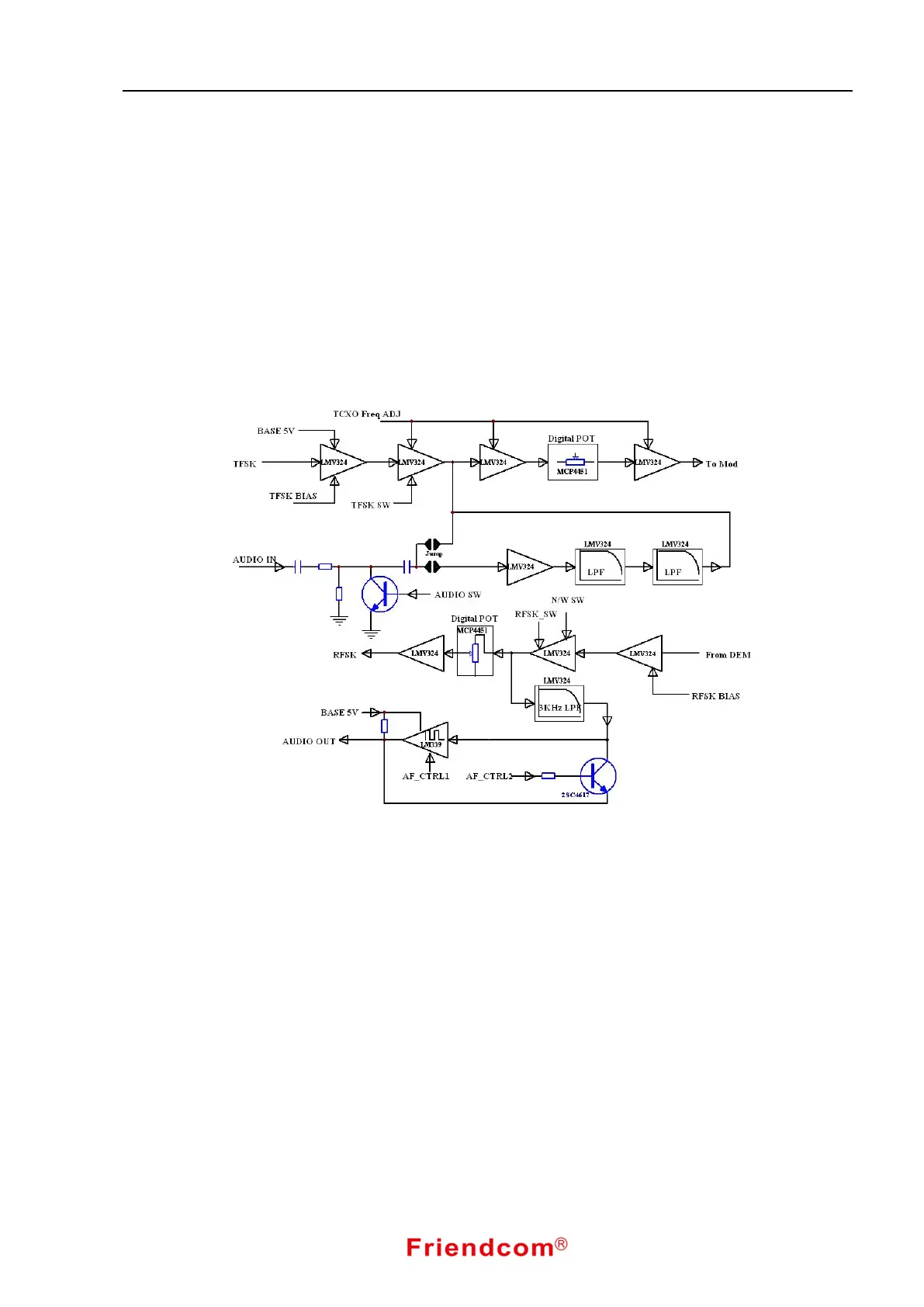
Fig. 4 Data Baseband Circuit Diagram
The circuit mainly works on the amplification of data base band signal, filtering of FSK baseband and
shaping etc.
The data baseband processing circuit supports very low signal frequency, even the DC level and the
amplitude frequency characteristics of wide and flat to meet the high-speed data transmission. The baseband
signal join from the TFSK end and is sent to the modulation circuit after DC level shift, amplification, channel
switch and a gain adjustment circuit .
AUDIO IN offer another data/voice modulation input port, which can transfer audio (data) signals sub
3KHz, adopting AC coupling with narrow frequency response, appropriate for low-speed data modulation.
In Rx mode, the intermediate frequency demodulation chip output baseband signal. The baseband signal is
amplified and go through DC level shift, narrowband and wideband switching, then is sent to the variable
gain amplifier. After that baseband signal containing DC component is output from the RFSK terminal. The
other signal is sent to the low pass filter to select sub 3KHz audio signal (data). After controllable switch circuit,
audio(data) output from filter or data signal shaped into a square wave signal can be output directly in AUDIO
OUT, appropriate for low speed data transmission.