Chapter 3 -- Instrument Circuitry--Reference 3000 Schematic/Block Diagrams
3 - 5
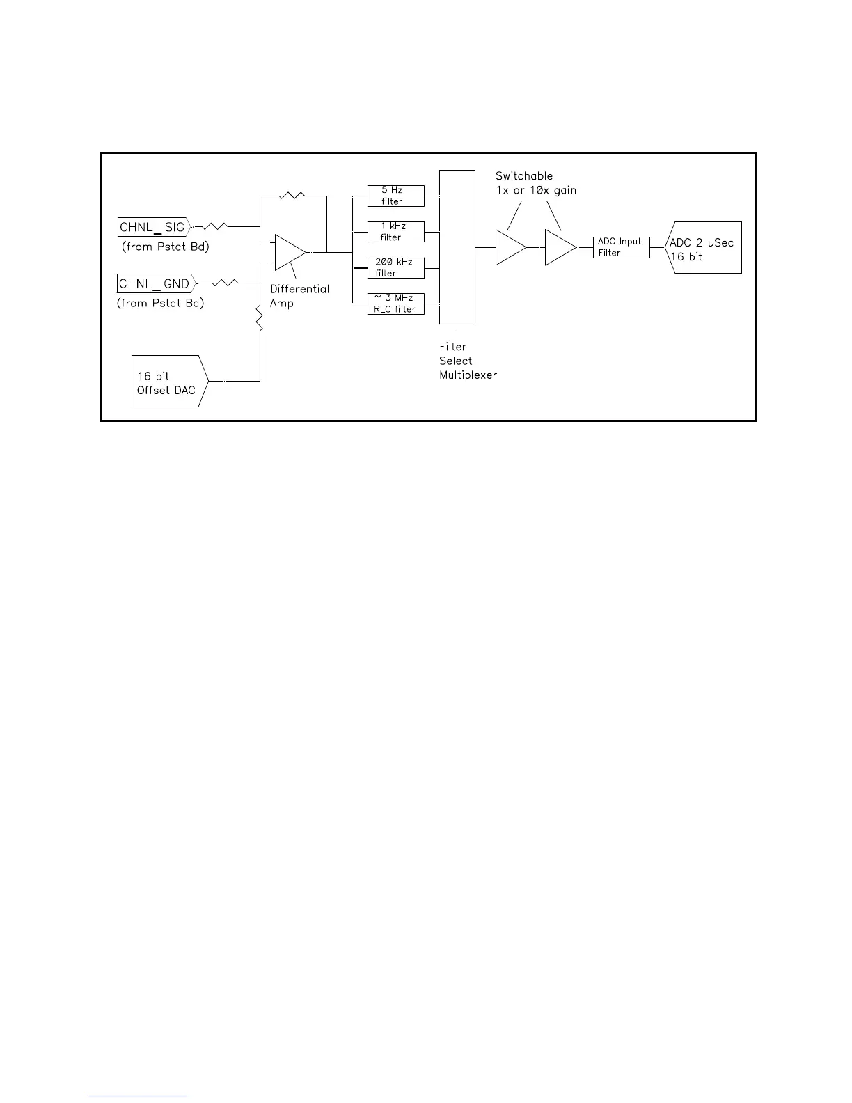
Figure 3-3
One A/D Signal Chain in the Reference 3000
Notes for Figure 3-3:
• This diagram shows one of three identical ADC channels. One channel is dedicated to measurement
of the potentiostat’s current signal, another is used to measure the cell or stack voltage, and the third is
switched between a wide selection of possible signals. See Figure 3-4
• All three A/D converters are triggered simultaneously to start a conversion. This trigger and the pulse
updating the Scan DAC voltage are under the control of a hardware state-machine. This insures that all
waveform and data acquisition timing is tightly controlled and reproducible point-to-point.
By default, the data acquisition is synchronized with the 300 kHz power supply switching frequency, to
reduce noise due to the power supply. Data acquisition times that are a multiple of 3.333 µSec will
maintain this synchronization.
• All analog signals that cross from the Potentiostat Board to the Control Board or vise versa are received
differentially as shown here.
• The 5 Hz, 1 kHz, and 200 kHz filters are 2-pole Butterworth filters. The 3 MHz RLC filter has an
arbitrary transfer function.
• All signal channel components are selected for optimal DC accuracy, low noise, and high bandwidth.