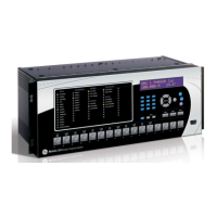
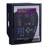
B-34 C60 Breaker Protection System GE Multilin
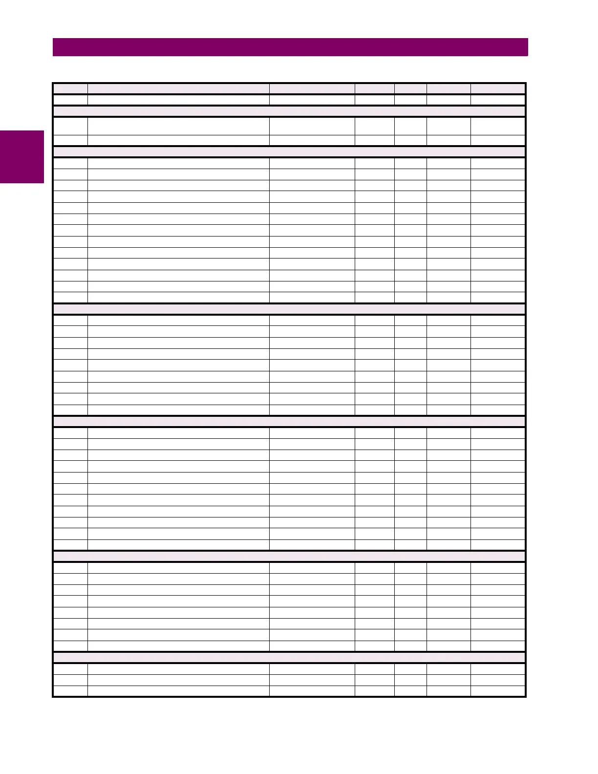
B.4 MEMORY MAPPING APPENDIX B
B
438E ...Repeated for Route 6
Installation (Read/Write Setting)
43E0 Relay Programmed State 0 to 1 --- 1 F133 0 (Not
Programmed)
43E1 Relay Name --- --- --- F202 “Relay-1”
User Programmable Self Tests (Read/Write Setting)
4441 User Programmable Detect Ring Break Function 0 to 1 --- 1 F102 1 (Enabled)
4442 User Programmable Direct Device Off Function 0 to 1 --- 1 F102 1 (Enabled)
4443 User Programmable Remote Device Off Function 0 to 1 --- 1 F102 1 (Enabled)
4444 User Programmable First Ethernet Fail Function 0 to 1 --- 1 F102 0 (Disabled)
4445 User Programmable Secondary Ethernet Fail Function 0 to 1 --- 1 F102 0 (Disabled)
4446 User Programmable Battery Fail Function 0 to 1 --- 1 F102 1 (Enabled)
4447 User Programmable SNTP Fail Function 0 to 1 --- 1 F102 1 (Enabled)
4448 User Programmable IRIG-B Fail Function 0 to 1 --- 1 F102 1 (Enabled)
4449 User Programmable Ethernet Switch Fail Function 0 to 1 --- 1 F102 1 (Enabled)
444A Process Bus Failure Operand 0 to 4294967295 --- 1 F300 0
444C PTP Fail Function 0 to 1 --- 1 F102 1 (Enabled)
444D User Programmable Third Ethernet Fail Function 0 to 1 --- 1 F102 0 (Disabled)
444E User Programmable SFP Fail Function 0 to 1 --- 1 F102 0 (Disabled)
CT Settings (Read/Write Setting) (6 modules)
4480 Phase CT 1 Primary 1 to 65000 A 1 F001 1
4481 Phase CT 1 Secondary 0 to 1 --- 1 F123 0 (1 A)
4482 Ground CT 1 Primary 1 to 65000 A 1 F001 1
4483 Ground CT 1 Secondary 0 to 1 --- 1 F123 0 (1 A)
4484 ...Repeated for CT Bank 2
4488 ...Repeated for CT Bank 3
448C ...Repeated for CT Bank 4
4490 ...Repeated for CT Bank 5
4494 ...Repeated for CT Bank 6
VT Settings (Read/Write Setting) (6 modules)
4500 Phase VT 1 Connection 0 to 1 --- 1 F100 0 (Wye)
4501 Phase VT 1 Secondary 25 to 240 V 0.1 F001 664
4502 Phase VT 1 Ratio 1 to 24000 :1 1 F060 1
4504 Auxiliary VT 1 Connection 0 to 6 --- 1 F166 1 (Vag)
4505 Auxiliary VT 1 Secondary 25 to 240 V 0.1 F001 664
4506 Auxiliary VT 1 Ratio 1 to 24000 :1 1 F060 1
4508 ...Repeated for VT Bank 2
4510 ...Repeated for VT Bank 3
4518 ...Repeated for VT Bank 4
4520 ...Repeated for VT Bank 5
4528 ...Repeated for VT Bank 6
Source Settings (Read/Write Setting) (4 modules)
4580 Source 1 Name 0 to 1 --- 1 F206 “SRC 1"
4583 Source 1 Phase CT 0 to 63 --- 1 F400 0
4584 Source 1 Ground CT 0 to 63 --- 1 F400 0
4585 Source 1 Phase VT 0 to 63 --- 1 F400 0
4586 Source 1 Auxiliary VT 0 to 63 --- 1 F400 0
4587 ...Repeated for Source 2
458E ...Repeated for Source 3
4595 ...Repeated for Source 4
Power System (Read/Write Setting)
4600 Nominal Frequency 25 to 60 Hz 1 F001 60
4601 Phase Rotation 0 to 1 --- 1 F106 0 (ABC)
4602 Frequency and Phase Reference 0 to 5 --- 1 F167 0 (SRC 1)
Table B–10: MODBUS MEMORY MAP (Sheet 26 of 66)
ADDR REGISTER NAME RANGE UNITS STEP FORMAT DEFAULT