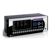
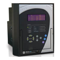
B-68 C60 Breaker Protection System GE Multilin
B.4 MEMORY MAPPING APPENDIX B
B
IEC 61850 GGIO2 Control Configuration (Read/Write Setting) (64 modules)
D320 IEC 61850 GGIO2.CF.SPCSO1.ctlModel Value 0 to 2 --- 1 F001 1
D321 IEC 61850 GGIO2.CF.SPCSO2.ctlModel Value 0 to 2 --- 1 F001 1
D322 IEC 61850 GGIO2.CF.SPCSO3.ctlModel Value 0 to 2 --- 1 F001 1
D323 IEC 61850 GGIO2.CF.SPCSO4.ctlModel Value 0 to 2 --- 1 F001 1
D324 IEC 61850 GGIO2.CF.SPCSO5.ctlModel Value 0 to 2 --- 1 F001 1
D325 IEC 61850 GGIO2.CF.SPCSO6.ctlModel Value 0 to 2 --- 1 F001 1
D326 IEC 61850 GGIO2.CF.SPCSO7.ctlModel Value 0 to 2 --- 1 F001 1
D327 IEC 61850 GGIO2.CF.SPCSO8.ctlModel Value 0 to 2 --- 1 F001 1
D328 IEC 61850 GGIO2.CF.SPCSO9.ctlModel Value 0 to 2 --- 1 F001 1
D329 IEC 61850 GGIO2.CF.SPCSO10.ctlModel Value 0 to 2 --- 1 F001 1
D32A IEC 61850 GGIO2.CF.SPCSO11.ctlModel Value 0 to 2 --- 1 F001 1
D32B IEC 61850 GGIO2.CF.SPCSO12.ctlModel Value 0 to 2 --- 1 F001 1
D32C IEC 61850 GGIO2.CF.SPCSO13.ctlModel Value 0 to 2 --- 1 F001 1
D32D IEC 61850 GGIO2.CF.SPCSO14.ctlModel Value 0 to 2 --- 1 F001 1
D32E IEC 61850 GGIO2.CF.SPCSO15.ctlModel Value 0 to 2 --- 1 F001 1
D32F IEC 61850 GGIO2.CF.SPCSO16.ctlModel Value 0 to 2 --- 1 F001 1
D330 IEC 61850 GGIO2.CF.SPCSO17.ctlModel Value 0 to 2 --- 1 F001 1
D331 IEC 61850 GGIO2.CF.SPCSO18.ctlModel Value 0 to 2 --- 1 F001 1
D332 IEC 61850 GGIO2.CF.SPCSO19.ctlModel Value 0 to 2 --- 1 F001 1
D333 IEC 61850 GGIO2.CF.SPCSO20.ctlModel Value 0 to 2 --- 1 F001 1
D334 IEC 61850 GGIO2.CF.SPCSO21.ctlModel Value 0 to 2 --- 1 F001 1
D335 IEC 61850 GGIO2.CF.SPCSO22.ctlModel Value 0 to 2 --- 1 F001 1
D336 IEC 61850 GGIO2.CF.SPCSO23.ctlModel Value 0 to 2 --- 1 F001 1
D337 IEC 61850 GGIO2.CF.SPCSO24.ctlModel Value 0 to 2 --- 1 F001 1
D338 IEC 61850 GGIO2.CF.SPCSO25.ctlModel Value 0 to 2 --- 1 F001 1
D339 IEC 61850 GGIO2.CF.SPCSO26.ctlModel Value 0 to 2 --- 1 F001 1
D33A IEC 61850 GGIO2.CF.SPCSO27.ctlModel Value 0 to 2 --- 1 F001 1
D33B IEC 61850 GGIO2.CF.SPCSO28.ctlModel Value 0 to 2 --- 1 F001 1
D33C IEC 61850 GGIO2.CF.SPCSO29.ctlModel Value 0 to 2 --- 1 F001 1
D33D IEC 61850 GGIO2.CF.SPCSO30.ctlModel Value 0 to 2 --- 1 F001 1
D33E IEC 61850 GGIO2.CF.SPCSO31.ctlModel Value 0 to 2 --- 1 F001 1
D33F IEC 61850 GGIO2.CF.SPCSO32.ctlModel Value 0 to 2 --- 1 F001 1
D340 IEC 61850 GGIO2.CF.SPCSO33.ctlModel Value 0 to 2 --- 1 F001 1
D341 IEC 61850 GGIO2.CF.SPCSO34.ctlModel Value 0 to 2 --- 1 F001 1
D342 IEC 61850 GGIO2.CF.SPCSO35.ctlModel Value 0 to 2 --- 1 F001 1
D343 IEC 61850 GGIO2.CF.SPCSO36.ctlModel Value 0 to 2 --- 1 F001 1
D344 IEC 61850 GGIO2.CF.SPCSO37.ctlModel Value 0 to 2 --- 1 F001 1
D345 IEC 61850 GGIO2.CF.SPCSO38.ctlModel Value 0 to 2 --- 1 F001 1
D346 IEC 61850 GGIO2.CF.SPCSO39.ctlModel Value 0 to 2 --- 1 F001 1
D347 IEC 61850 GGIO2.CF.SPCSO40.ctlModel Value 0 to 2 --- 1 F001 1
D348 IEC 61850 GGIO2.CF.SPCSO41.ctlModel Value 0 to 2 --- 1 F001 1
D349 IEC 61850 GGIO2.CF.SPCSO42.ctlModel Value 0 to 2 --- 1 F001 1
D34A IEC 61850 GGIO2.CF.SPCSO43.ctlModel Value 0 to 2 --- 1 F001 1
D34B IEC 61850 GGIO2.CF.SPCSO44.ctlModel Value 0 to 2 --- 1 F001 1
D34C IEC 61850 GGIO2.CF.SPCSO45.ctlModel Value 0 to 2 --- 1 F001 1
D34D IEC 61850 GGIO2.CF.SPCSO46.ctlModel Value 0 to 2 --- 1 F001 1
D34E IEC 61850 GGIO2.CF.SPCSO47.ctlModel Value 0 to 2 --- 1 F001 1
D34F IEC 61850 GGIO2.CF.SPCSO48.ctlModel Value 0 to 2 --- 1 F001 1
D350 IEC 61850 GGIO2.CF.SPCSO49.ctlModel Value 0 to 2 --- 1 F001 1
D351 IEC 61850 GGIO2.CF.SPCSO50.ctlModel Value 0 to 2 --- 1 F001 1
D352 IEC 61850 GGIO2.CF.SPCSO51.ctlModel Value 0 to 2 --- 1 F001 1
D353 IEC 61850 GGIO2.CF.SPCSO52.ctlModel Value 0 to 2 --- 1 F001 1
D354 IEC 61850 GGIO2.CF.SPCSO53.ctlModel Value 0 to 2 --- 1 F001 1
Table B–10: MODBUS MEMORY MAP (Sheet 60 of 66)
ADDR REGISTER NAME RANGE UNITS STEP FORMAT DEFAULT