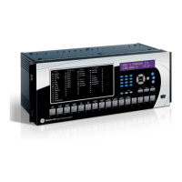
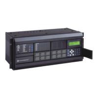
B-36 G60 Generator Protection System GE Multilin
B.4 MEMORY MAPPING APPENDIX B
B
5C04 Neutral Instantaneous Overcurrent 1 Reset Delay 0 to 600 s 0.01 F001 0
5C05 Neutral Instantaneous Overcurrent 1 Block 0 to 4294967295 --- 1 F300 0
5C07 Neutral Instantaneous Overcurrent 1 Target 0 to 2 --- 1 F109 0 (Self-reset)
5C08 Neutral Instantaneous Overcurrent 1 Events 0 to 1 --- 1 F102 0 (Disabled)
5C09 Reserved (8 items) 0 to 1 --- 1 F001 0
Ground Time Overcurrent (Read/Write Grouped Setting) (1 module)
5D00 Ground Time Overcurrent 1 Function 0 to 1 --- 1 F102 0 (Disabled)
5D01 Ground Time Overcurrent 1 Signal Source 0 to 5 --- 1 F167 0 (SRC 1)
5D02 Ground Time Overcurrent 1 Input 0 to 1 --- 1 F122 0 (Phasor)
5D03 Ground Time Overcurrent 1 Pickup 0 to 30 pu 0.001 F001 1000
5D04 Ground Time Overcurrent 1 Curve 0 to 16 --- 1 F103 0 (IEEE Mod Inv)
5D05 Ground Time Overcurrent 1 Multiplier 0 to 600 --- 0.01 F001 100
5D06 Ground Time Overcurrent 1 Reset 0 to 1 --- 1 F104 0 (Instantaneous)
5D07 Ground Time Overcurrent 1 Block 0 to 4294967295 --- 1 F300 0
5D09 Ground Time Overcurrent 1 Target 0 to 2 --- 1 F109 0 (Self-reset)
5D0A Ground Time Overcurrent 1 Events 0 to 1 --- 1 F102 0 (Disabled)
5D0B Reserved (6 items) 0 to 1 --- 1 F001 0
Ground Instantaneous Overcurrent (Read/Write Grouped Setting) (1 module)
5DA0 Ground Instantaneous Overcurrent 1 Function 0 to 1 --- 1 F102 0 (Disabled)
5DA1 Ground Instantaneous Overcurrent 1 Signal Source 0 to 5 --- 1 F167 0 (SRC 1)
5DA2 Ground Instantaneous Overcurrent 1 Pickup 0 to 30 pu 0.001 F001 1000
5DA3 Ground Instantaneous Overcurrent 1 Delay 0 to 600 s 0.01 F001 0
5DA4 Ground Instantaneous Overcurrent 1 Reset Delay 0 to 600 s 0.01 F001 0
5DA5 Ground Instantaneous Overcurrent 1 Block 0 to 4294967295 --- 1 F300 0
5DA7 Ground Instantaneous Overcurrent 1 Target 0 to 2 --- 1 F109 0 (Self-reset)
5DA8 Ground Instantaneous Overcurrent 1 Events 0 to 1 --- 1 F102 0 (Disabled)
5DA9 Reserved (8 items) 0 to 1 --- 1 F001 0
CT Fail (Read/Write Setting) (6 modules)
5E6C CT Fail 1 Function 0 to 1 --- 1 F102 0 (Disabled)
5E6D CT Fail 1 Block 0 to 4294967295 --- 1 F300 0
5E6F CT Fail 1 Current Source 1 0 to 5 --- 1 F167 0 (SRC 1)
5E70 CT Fail 1 Current Pickup 1 0 to 2 pu 0.1 F001 2
5E71 CT Fail 1 Current Source 2 0 to 5 --- 1 F167 1 (SRC 2)
5E72 CT Fail 1 Current Pickup 2 0 to 2 pu 0.1 F001 2
5E73 CT Fail 1 Voltage Source 0 to 5 --- 1 F167 0 (SRC 1)
5E74 CT Fail 1 Voltage Pickup 0 to 2 pu 0.01 F001 20
5E75 CT Fail 1 Pickup Delay 0 to 65.535 s 0.001 F001 1000
5E76 CT Fail 1 Target 0 to 2 --- 1 F109 0 (Self-reset)
5E77 CT Fail 1 Events 0 to 1 --- 1 F102 0 (Disabled)
5E78 ...Repeated for CT Fail 2
5E84 ...Repeated for CT Fail 3
5E90 ...Repeated for CT Fail 4
5E9C ...Repeated for CT Fail 5
5EA8 ...Repeated for CT Fail 6
Frequency Out-Of-Band Accumulation (Read/Write Setting)
5F40 Frequency Out-Of-Band Accumulation Block 0 to 4294967295 --- 1 F300 0
5F42 Frequency Out-Of-Band Accumulation Events Enable 0 to 1 --- 1 F102 0 (Disabled)
5F43 Frequency Out-Of-Band Accumulator Function Enable
Array (7 items)
0 to 1 --- 1 F102 0 (Disabled)
5F4A Frequency Out-Of-Band Accumulator Lower Frequency
Array (7 items)
20 to 70 Hz 0.01 F001 6000
5F51 Frequency Out-Of-Band Accumulator Min Value V A 0.1 to 1.25 pu 0.01 F001 10
5F52 Frequency Out-Of-Band Accumulator Source 0 to 5 --- 1 F167 0 (SRC 1)
5F53 Frequency Out-Of-Band Accumulator Target Messages
Enable
0 to 2 --- 1 F109 0 (Self-reset)
Table B–10: MODBUS MEMORY MAP (Sheet 28 of 68)
ADDR REGISTER NAME RANGE UNITS STEP FORMAT DEFAULT
 Loading...