Confidential & Proprietary Information
5
HARDWARE LAYOUT/REFERENCE DESIGN
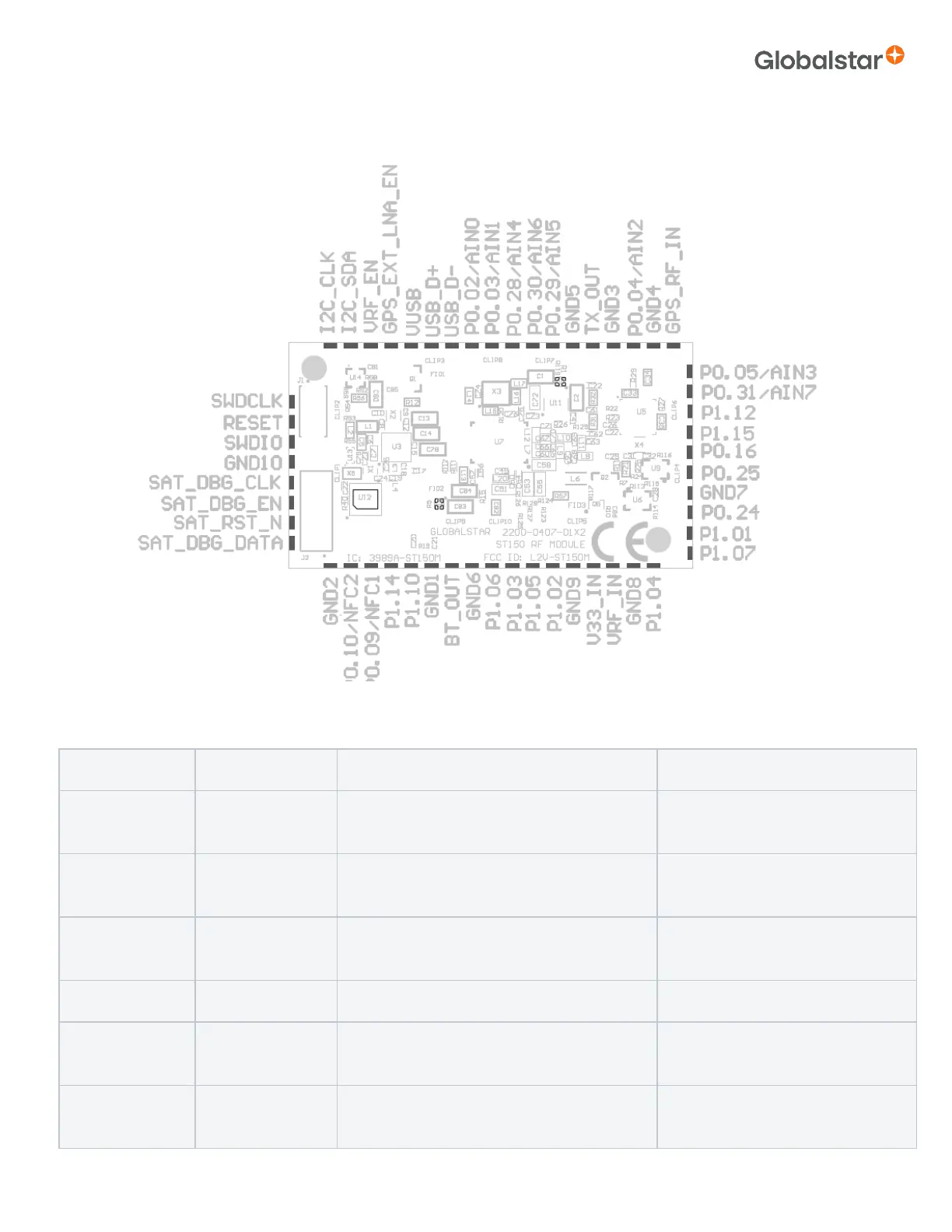
5.1 PIN ASSIGNMENTS
Pin Function Description Recommended Usage
SWDCLK Debug
Serial wire debug clock input for Nordic
debug and programming
3.3V level
RESET Debug
Reset input for Nordic debug and
programming
3.3V level
SWDIO Debug
Serial wire debug I/O for debug and
programming
3.3V level
GND10 Power Ground –
SAT_DBG_CLK Debug
Serial wire debug clock input for ASIC
debug and programming
3V level
SAT_DBG_EN Debug
Debug enable input for ASIC debug and
programming
3V level
FIGURE 5 – PIN ASSIGNMENTS