1-6
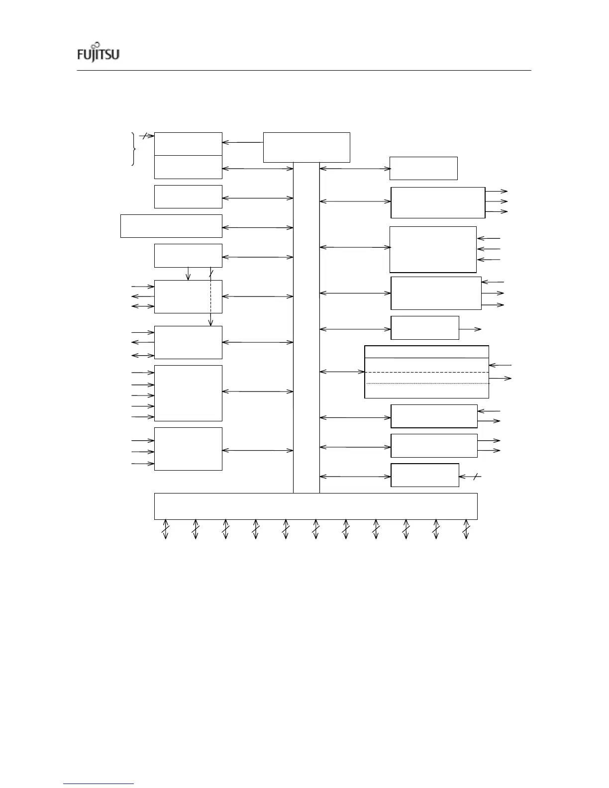
Fig. 1.1 Block Diagram (MB90470)
P00 to P07 (8): Provided with input pull-up resistor setting register
P10 to P17 (8): Provided with input pull-up resistor setting register
P40 to P47 (8): Provided with open-drain setting register
P70 to P75 (6): Provided with open-drain setting register
P76 to P77 (2): Open-drain
Note: In the figure above, the I/O port shares the pins with each internal functional block. When the pins
are used as internal module pins, they cannot be used as I/O port pins.
X0, X1 RSTX
X0, X1A
5
CPU
F
2
MC-16LX family
core
Communication
prescaler
UART
A/D converter
(10 bits)
I/O expanded
serial
interface x 2
channels
SIN1, 2
SOT1, 2
SCK1, 2
AVCC
AVRH. L
AVSS
ADTG
AN0 to 7
Interrupt controller
8-/16-bit PPG
PPG0, 1
PPG2, 3
PPG4, 5
8-/16-bits UD counter
IN0, 1
OUT0, 1, 2,
3, 4, 5
16-bit reload timer
x 2 channels
TIN0
TOT0
External interrupt
IRQ0 to 7
8
I/O timer
16-bit input capture x 2
16-bit output conveyer x 6
16-bit free-run timer
I
2
C interface
SCL
SDA
I/O port
µ
PG
P00 P10 P20 P30 P40 P50 P60 P70 P80 P90 PA0
P07 P17 P27 P37 P47 P57 P67 P77 P87 P97 PA3
888 88 88 88 8 4
AIN0, 1
BIN0, 1
ZIN0, 1
EXTC
MT00
MT01
16-bit PWC
3 channels
PWC0
PWC1
PWC2
Chip select
CS0, 1, 2, 3
2
Clock control
circuit
RAM
ROM
EI
2
OS
SIN0
SOT0
SCK0

 Loading...