HY57V161610ETP-I
2 Banks x 512K x 16 Bit Synchronous DRAM
This document is a general product description and is subject to change without notice. Hynix Semiconductor does not assume any responsibility for
use of circuits described. No patent licenses are implied
Rev. 0.1 / Nov. 2003 1
DESCRIPTION
THE Hynix HY57V161610E is a 16,777,216-bits CMOS Synchronous DRAM, ideally suited for the main memory and graphic appli-
cations which require large memory density and high bandwidth. HY57V161610E is organized as 2banks of 524,288x16.
HY57V161610E is offering fully synchronous operation referenced to a positive edge clock. All inputs and outputs are synchronized
with the rising edge of the clock input. The data paths are internally pipelined to achieve very high bandwidth. All input and output
voltage levels are compatible with LVTTL.
Programmable options include the length of pipeline (Read latency of 1,2 or 3), the number of consecutive read or write cycles initi-
ated by a single control command (Burst length of 1,2,4,8 or full page), and the burst count sequence(sequential or interleave). A
burst of read or write cycles in progress can be terminated by a burst terminate command or can be interrupted and replaced by a
new burst read or write command on any cycle. (This pipeline design is not restricted by a `2N` rule.)
FEATURES
• Single 3.0V to 3.6V power supply
• All device pins are compatible with LVTTL interface
• JEDEC standard 400mil 50pin TSOP-II with 0.8mm of pin
pitch
• All inputs and outputs referenced to positive edge of system
clock
• Data mask function by UDQM/LDQM
• Internal two banks operation
• Auto refresh and self refresh
• 4096 refresh cycles / 64ms
• Programmable Burst Length and Burst Type
- 1, 2, 4, 8 and Full Page for Sequence Burst
- 1, 2, 4 and 8 for Interleave Burst
• Programmable CAS Latency ; 1, 2, 3 Clocks
• Pb-free Package
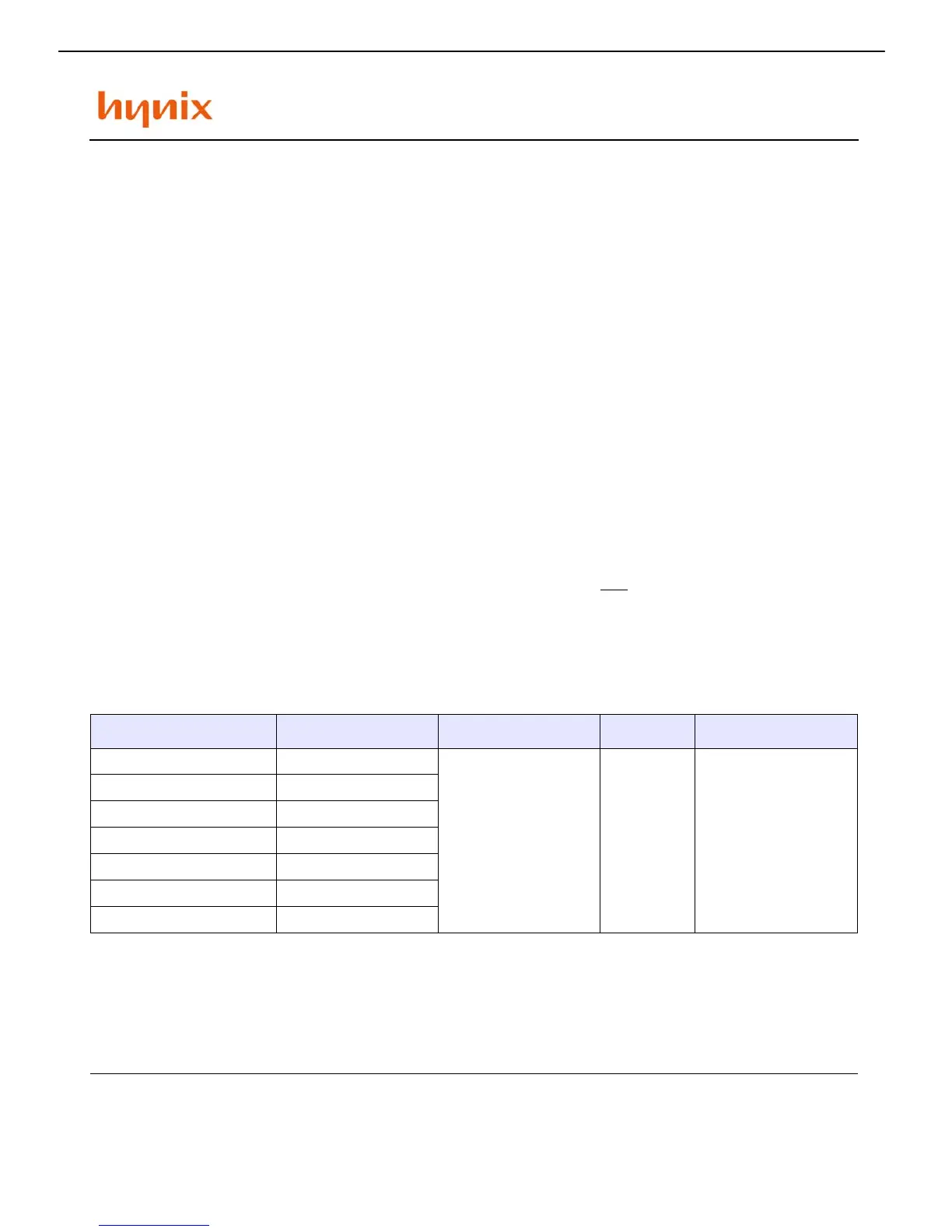
ORDERING INFORMATION
Part No. Clock Frequency Organization Interface Package
HY57V161610ETP-5I 200MHz
2Banks x 512Kbits x 16 LVTTL
400mil
50pin TSOP II
(Pb free)
HY57V161610ETP-55I 183MHz
HY57V161610ETP-6I 166MHz
HY57V161610ETP-7I 143MHz
HY57V161610ETP-8I 125MHz
HY57V161610ETP-10I 100MHz
HY57V161610ETP-15I 66MHz
Note :
1. VDD(min) of HY57V161610ETP-5I/55I is 3.15V
2. Hynix supports lead free part for each speed grade with same specification.

 Loading...