HT48R07A-1/HT48C07, HT48R09A-1/HT48C09
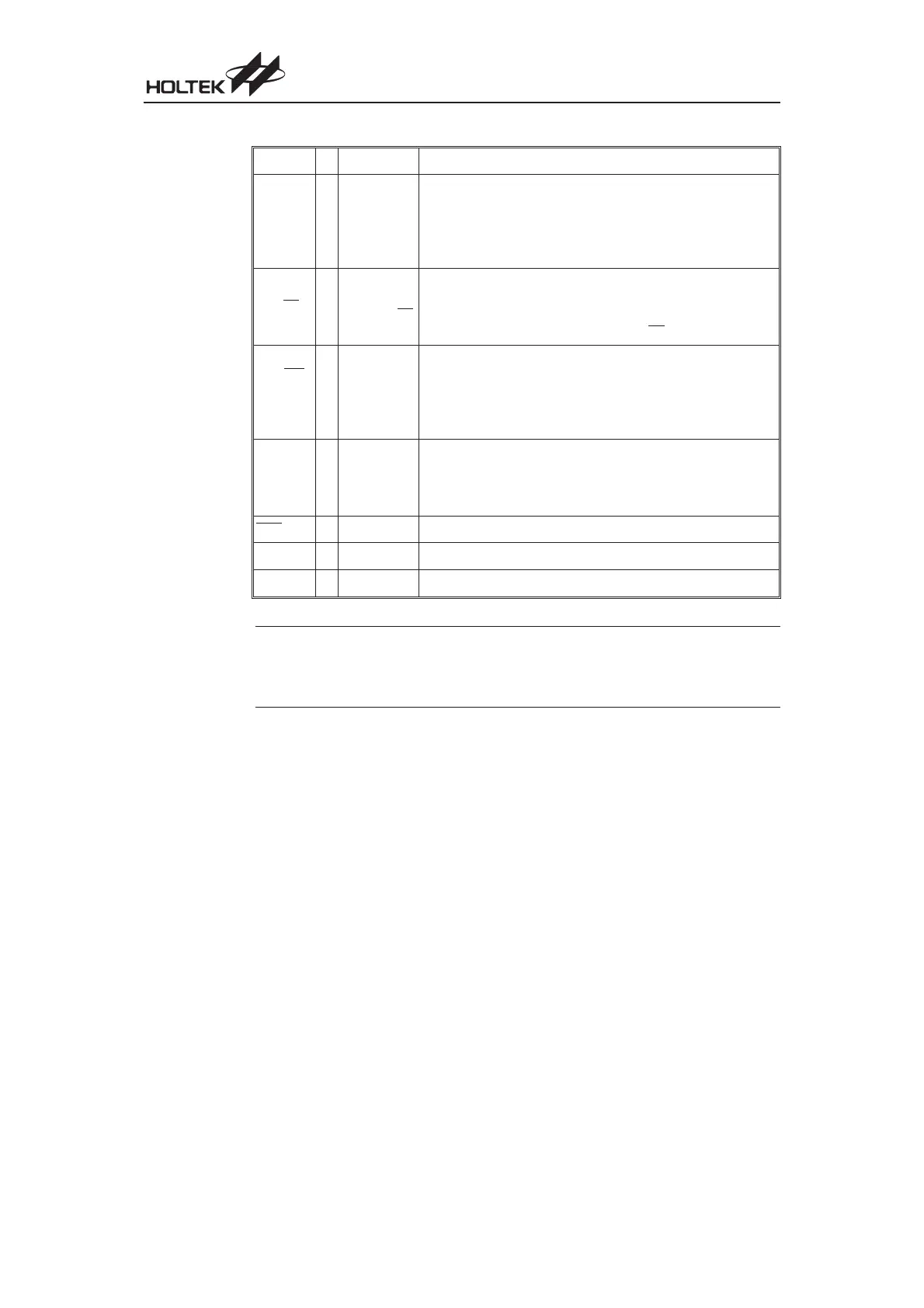
Pin Name I/O Options Description
PA0~PA7 I/O
Pull-high
Wake-up
Bidirectional 8-bit input/output port. Each individual bit on this port
can be configured as a wake-up input by a configuration option.
Software instructions determine if the pin is a CMOS output or
Schmitt Trigger input. A configuration option determines if all pins
on this port have pull-high resistors.
PB0/BZ
PB1/BZ
PB2~PB7
I/O
Pull-high
I/O or BZ/BZ
Bidirectional 8-bit input/output port. Software instructions determine
if the pin is a CMOS output or Schmitt Trigger input. A configuration
option determines if all pins on this port have pull-high resistors.
PB0 and PB1 are pin-shared with BZ and BZ
, respectively.
PC0/INT
PC1/TMR
PC2
I/O Pull-high
Bidirectional 3-bit input/output port. Software instructions deter
-
mine if the pin is a CMOS output or Schmitt Trigger input. A config
-
uration option determines if all pins on this port have pull-high
resistors. The external interrupt and timer input are pin-shared
with PC0 and PC1, respectively.
OSC1
OSC2
I
O
Crystal or RC
OSC1, OSC2 are connected to an external RC network or external
crystal (determined by configuration option) for the internal system
clock. For external RC system clock operation, OSC2 is an output
pin for 1/4 system clock.
RES I
¾
Schmitt
Trigger reset input. Active low.
VDD
¾¾
Positive power supply
VSS
¾¾
Negative power supply, ground
Note 1. Each pin on PA can be programmed through a configuration option to have a wake-up function.
2. Individual pins cannot be selected to have pull-high resistors. If the pull-high configuration is
chosen for a particular port, then all input pins on this port will be connected to pull-high resis-
tors.
Absolute Maximum Ratings
Supply Voltage.............................................................................................V
SS
-0.3V to V
SS
+6.0V
Input Voltage ...............................................................................................V
SS
-0.3V to V
DD
+0.3V
Storage Temperature.............................................................................................-50°Cto125°C
Operating Temperature............................................................................................-40°Cto85°C
These are stress ratings only. Stresses exceeding the range specified under Absolute Maximum
Ratings may cause substantial damage to the device. Functional operation of this device at other
conditions beyond those listed in the specification is not implied and prolonged exposure to ex
-
treme conditions may affect device reliability.
8
Cost-Effective I/O Type MCU
 Loading...