Honeywell
COMPONENT MAINTENANCE MANUAL
PART NUMBER 964-0452
I.B.1516A Page 55
Mar 30/01
23-12-01
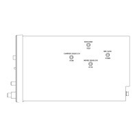
Block Diagram, ARINC Input
Figure 31
A pause of at least 3 bits between the OR clock pulse is detected by the pause
recognition circuit. The 32-bit ARINC word is reloaded from the shift register in
a 32-bit holding register with the positive edge of the circuit, and an interrupt
flip-flop is set. This flip-flop is reset by a read cycle to the holding register.
2 ARINC output
ARINC output is composed of 3 function blocks. The 32-bit shift register is load-
ed in parallel via the processor bus. The shift clock-pulse generator generates
all the clock signals necessary for shift purposes. The multiplexer finally gener-
ates the ARINC bipolar RZ ARINC signal from the signals of the shift register
and the clock-pulse generator.
The 50kHz C50kHz rectangular signal is supplied to the clock-pulse generator.
If a positive pulse is issued to the START line, the clock-pulse generator produc-
es 32 write pulses for the shift register. The clock-pulse generator counts on 6
bits and sets the INTOT line via an interrupt flip-flop. This line in turn generates
an interrupt, thus signalling that a further data word can be sent. The INTOT line
is reset by a pulse on the START line.
Analog multiplexer D21 generates the ARINC signal from the data and the shift
register clock-pulse. The differential output signals (referred to the ground of the
transmitter) are defined as:
Level of Differential Output Signals
Figure 32
HI ZERO LOW
Line A to B +10 ± 1.0V 0 ± 0.50V –10 ± 1.0V
Line A to Ground +5 ± 0.5V 0 ± 0.25V –5 ± 0.5V
Line B to Ground –5 ± 0.5V 0 ± 0.25V +5 ± 0.5V
Page 83
 Loading...