Honeywell
COMPONENT MAINTENANCE MANUAL
PART NUMBER 964-0452
1I.B.1516A Page 56
Mar 30/01
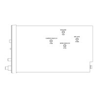
23-12-01
Block Diagram, ARINC Output
Figure 33
3 Parallel output
Open-collector transistor, V4, is controlled via a port output on module, D3. This
generates the KEYEV signal.
4 Parallel input
The Logic states of discrete input lines can be inquired by input port modules,
D1 and D2. These input lines can also generate a pulse during the transition
from LOW-to-HIGH and from HIGH-to-LOW, which is forwarded to an interrupt
input from the processor:
– TUNPOW
– KYINTL
– VOIDA
– BITKEY
Debounced PTT input Lines, CPTT, DATON, CWON, are available for delayed
suitching on the radio. Depending upon the current modulation type, 1 of the 3
inputs is connected through to the debouncing circuit in each case.
The debouncing circuit is provided by monoflop, D4. Monoflop, D4-A, is trig-
gered by the first negative edge of the bouncing PTT signal. The negative pulse
at NAND gate, D32-A, suppresses the bounce pulses of the button. If the PTT
button is released, monoflop, D32-B, is triggered. Any bounce pulses are now
suppressed by a negative pulse at NAND gate, D32-B. Both monoflops are set
to pulse widths of 20ms by means of an R-C combination.
Page 84
 Loading...