EasyManua.ls Logo

Icom IC-275H Service Manual

Icom IC-275H
135 pages
To Next Page IconTo Next Page
Page #1 background imageLoading...
Page #1 background image

Other manuals for Icom IC-275H

Question and Answer IconNeed help?

Do you have a question about the Icom IC-275H and is the answer not in the manual?

Icom IC-275H Specifications

General IconGeneral
Frequency Range144-148 MHz
ModeFM
Receiver Sensitivity0.2 µV (12 dB SINAD)
Supply Voltage13.8 V DC
Sensitivity0.16 μV for 12 dB SINAD

Summary

Scope of the Service Manual

Assistance

Guidance on obtaining help for operation, capability, and servicing from ICOM.

Ordering Replacement Parts

Information on how to order parts for efficient service.

Section 1 Specifications

Frequency Coverage

Specifies the frequency ranges for different versions of the transceiver.

Power Supply Requirement

Outlines the voltage and current requirements for the power supply.

Transmitter Specifications

Details specifications related to the transmitter functionality.

Receiver Specifications

Receive System

Describes the receiver system architecture.

Sensitivity (with a 50Ω Load)

Details the receiver sensitivity with a 50-ohm load.

Selectivity

Details the receiver selectivity characteristics.

Section 2 Outside and Inside Views

2-1 Front Panel

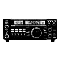
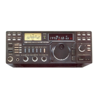
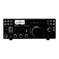
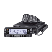
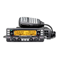
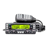
Explains the front panel layout and controls.

2-1-1 Front Panel Details

Detailed view and labeling of the front panel components.

2-1 Front Panel (Continued)

Frequency Display

Details the frequency display and its indicators.

2-1-3 Rear Panel

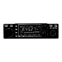
Explains the rear panel layout and connectors.

2-1-2 Inside Views

2-2-1 PLL and Logic Units

Shows the internal view of PLL and Logic units.

2-2-2 Main and RF YGR Units

Shows internal view of Main and RF YGR units.

Section 3 Block Diagrams

IC-275A/E/H Block Diagram

Block diagram for IC-275A/E/H models.

Section 4 Circuit Description

4-1 Receiver Circuits

Details on the receiver circuits of the transceiver.

4-1-1 Antenna - 1st Mixer Circuit

Details the antenna and 1st mixer circuit functionality.

Section 4 Circuit Description (Continued)

4-1-2 Noise Blanker, Notch Filter, FM Detector

Details on noise blanker, notch filter, and FM detector circuits.

4-1-3 SSB/CW Mixer Circuit and AF Amplifier

Description of mixer and AF amplifier circuits for SSB/CW.

Section 4 Circuit Description (Continued)

4-1-4 FM, Squelch, S-Meter, and Center Meter Circuits

Description of FM squelch, S-meter, and center meter circuits.

4-2 Transmitter Circuits

Details on the transmitter circuits of the transceiver.

Section 4 Circuit Description (Continued)

4-2-2 CW Mode Transmit IF Signals

Description of circuitry for CW mode transmit IF signals.

4-2-3 TX Amp/Antenna (IC-275A/E)

Description of TX Amp and Antenna circuits for IC-275A/E.

Section 4 Circuit Description (Continued)

4-3 Standby Control Circuit

Description of the standby control circuit.

Section 4 Circuit Description (Continued)

4-4 PLL Circuits

Description of the Phase Locked Loop (PLL) circuits.

Section 4 Circuit Description (Continued)

Section 4 Circuit Description (Continued)

4-5 Logic Circuits

Description of the logic circuits.

4-5-2 Reset Circuit

Description of the reset circuit.

Section 4 Circuit Description (Continued)

4-5-3 Sensor Circuit

Description of the sensor circuit.

4-5-5 Matrix

Explanation of the matrix used for controls.

Section 4-6 Switching Regulator Circuit (IC-275A/E Only)

Section 5 Mechanical Parts and Disassembly

5-1 Frame Disassembly

Steps for disassembling the transceiver frame.

Section 5 Mechanical Parts and Disassembly (Continued)

5-2 Front Panel Disassembly

Steps for disassembling the front panel.

Section 5 Mechanical Parts and Disassembly (Continued)

5-3 Rear Panel Disassembly

Steps for disassembling the rear panel.

Section 5 Mechanical Parts and Disassembly (Continued)

5-4 Front, Logic and PLL Units Connector Assembly

Connector assembly for front, logic, and PLL units.

Section 5 Mechanical Parts and Disassembly (Continued)

5-5 Front, Main and RF YGR Units Connector Assembly

Connector assembly for front, main, and RF YGR units.

Section 5 Mechanical Parts and Disassembly (Continued)

5-6 PA and REG Units Connector Assembly (IC-275A/E)

Connector assembly for PA and REG units (IC-275A/E).

Section 5 Mechanical Parts and Disassembly (Continued)

5-7 PA, CTRL and Filter Units Connector Assembly (IC-275H)

Connector assembly for PA, CTRL, and Filter units (IC-275H).

Section 6 Maintenance and Adjustment

6-1 Preparation Before Servicing

Important precautions before performing maintenance or servicing.

Section 6 Maintenance and Adjustment (Continued)

6-2 PLL Adjustment

Test instruments and locations for PLL adjustment.

Section 6 Maintenance and Adjustment (Continued)

6-3 Frequency and Tone Adjustment

Test instruments, locations, and values for frequency/tone adjustment.

Section 6 Maintenance and Adjustment (Continued)

Logic Unit Adjustments

Shows adjustment points on the logic unit.

Section 6 Maintenance and Adjustment (Continued)

6-4 Receiver Adjustment

Test instruments, locations, and values for receiver adjustment.

Section 6 Maintenance and Adjustment (Continued)

Receiver Adjustment (Continued)

Continuation of receiver adjustments.

Section 6 Maintenance and Adjustment (Continued)

6-5 Transmitter Adjustment (IC-275H)

Test instruments and conditions for transmitter adjustment.

Section 6 Maintenance and Adjustment (Continued)

Transmitter Adjustment (IC-275H) (Continued)

Continuation of transmitter adjustments.

Section 6 Maintenance and Adjustment (Continued)

6-6 Transmitter Adjustment (IC-275A/E)

Test instruments and conditions for transmitter adjustment.

Section 6 Maintenance and Adjustment (Continued)

Transmitter Adjustment (IC-275A/E) (Continued)

Continuation of transmitter adjustments.

Section 7 Board Layouts

7-1 Front Panel Units (1)

Component layout for Front Units (1).

Section 7 Board Layouts (Continued)

Front (SW-A) Unit

Component layout for Front (SW-A) Unit.

Front (VR-A) Unit

Component layout for Front (VR-A) Unit.

Section 7 Board Layouts (Continued)

7-2 Front Unit (2)

Component layout for Front Unit (2).

Section 7 Board Layouts (Continued)

Front Unit Components Side

Component placement on the front unit's component side.

Section 7 Board Layouts (Continued)

7-3 Logic and Sensor Units

Component details for logic and sensor units.

Section 7 Board Layouts (Continued)

Logic Unit PCB Layout

PCB layout and component connections for the logic unit.

Section 7 Board Layouts (Continued)

7-4 PLL and DDS Units

Component details for PLL and DDS units.

Section 7 Board Layouts (Continued)

PLL Unit PCB Layout

PCB layout and component connections for the PLL unit.

Section 7 Board Layouts (Continued)

DDS Unit Component Details

Component details and PCB layout for the DDS unit.

Section 7 Board Layouts (Continued)

7-5 Main Unit Components

Component details for the main unit.

Section 7 Board Layouts (Continued)

Main Unit PCB Layout

PCB layout and component connections for the main unit.

Section 7 Board Layouts (Continued)

7-6 RF YGR Unit

Component details and PCB layout for the RF YGR unit.

Section 7 Board Layouts (Continued)

7-7 REG Unit (IC-275A/E Only)

Component details for the REG unit (IC-275A/E).

Section 7 Board Layouts (Continued)

7-8 PA Unit (IC-275A/E)

Component details for the PA unit (IC-275A/E).

Section 7 Board Layouts (Continued)

7-9 CTRL Unit (IC-275H Only)

Component details for the CTRL unit (IC-275H).

Section 7 Board Layouts (Continued)

7-10 PA Unit (IC-275H)

Component details for the PA unit (IC-275H).

Section 7 Board Layouts (Continued)

7-11 Filter Unit (IC-275H Only)

Component details and PCB layout for the FILTER unit (IC-275H).

Section 8 Voltage Diagrams

8-1 Front Unit Voltage Diagram

Voltage diagram for the front unit.

Section 8 Voltage Diagrams (Continued)

8-2 Logic Unit Voltage Diagram

Voltage diagram for the logic unit.

Section 8 Voltage Diagrams (Continued)

8-3 PLL Unit Voltage Diagram

Voltage diagram for the PLL unit.

Section 8 Voltage Diagrams (Continued)

8-4 Main Unit Voltage Diagram

Voltage diagram for the main unit.

Section 8 Voltage Diagrams (Continued)

8-5 RF YGR Unit Voltage Diagram

Voltage diagram for the RF YGR unit.

Section 8 Voltage Diagrams (Continued)

8-6 REG and PA Units Voltage Diagrams (IC-275A/E Only)

Voltage diagrams for REG and PA units (IC-275A/E).

Section 8 Voltage Diagrams (Continued)

8-7 CTRL, PA and Filter Units Voltage Diagrams (IC-275H Only)

Voltage diagrams for CTRL, PA, and FILTER units (IC-275H).

Section 9 Parts List

EF Parts List

List of EF parts.

Front Unit Parts List

List of parts for the front unit.

Section 9 Parts List (Continued)

Reference Unit Parts List

List of parts for reference units.

Logic Unit Parts List

List of parts for the logic unit.

Section 9 Parts List (Continued)

Logic Unit Parts List (Continued)

Continuation of logic unit parts list.

PLL Unit Parts List

List of parts for the PLL unit.

Section 9 Parts List (Continued)

Main Unit Parts List

List of parts for the main unit.

Section 9 Parts List (Continued)

Main Unit Parts List (Continued)

Continuation of main unit parts list.

Section 9 Parts List (Continued)

Main Unit Parts List (Continued)

Continuation of main unit parts list.

SQL Unit Parts List

List of parts for the SQL unit.

Section 9 Parts List (Continued)

RF YGR Unit Parts List

List of parts for the RF YGR unit.

Section 9 Parts List (Continued)

REG Unit Parts List (IC-275A/E Only)

List of parts for the REG unit (IC-275A/E).

Section 9 Parts List (Continued)

PA Unit Parts List (IC-275A/E)

List of parts for the PA unit (IC-275A/E).

Section 9 Parts List (Continued)

CTRL Unit Parts List (IC-275H Only)

List of parts for the CTRL unit (IC-275H).

Section 9 Parts List (Continued)

Filter Unit Parts List (IC-275H Only)

List of parts for the FILTER unit (IC-275H).

IC-275H Schematic Diagram

Front Schematic

Schematic diagram of the front section.

Sensor Schematic

Schematic diagram of the sensor section.

Logic Schematic

Schematic diagram of the logic section.

Tone SQL Schematic

Schematic diagram of the tone SQL section.

Voice Schematic

Schematic diagram of the voice section.

IC-275H Schematic Diagram (Continued)

RAM Schematic

Schematic diagram of the RAM section.

IC-275H Schematic Diagram (Continued)

Main Schematic

Schematic diagram of the main section.

IC-275H Schematic Diagram (Continued)

Ctrl Schematic

Schematic diagram of the CTRL section.

Filter Schematic

Schematic diagram of the FILTER section.

PA Schematic

Schematic diagram of the PA section.

RF YGR Schematic

Schematic diagram of the RF YGR section.

IC-275H Schematic Diagram (Continued)

Logic Schematic

Schematic diagram of the logic section.

IC-275H Schematic Diagram (Continued)

DDS Schematic

Schematic diagram of the DDS section.

IC-275H Schematic Diagram (Continued)

PLL Schematic

Schematic diagram of the PLL section.

RF YGR Schematic

Schematic diagram of the RF YGR section.

IC-275A/E Schematic Diagram

Front Schematic

Schematic diagram of the front section.

Sensor Schematic

Schematic diagram of the sensor section.

Logic Schematic

Schematic diagram of the logic section.

Tone SQL Schematic

Schematic diagram of the tone SQL section.

Voice Schematic

Schematic diagram of the voice section.

IC-275A/E Schematic Diagram (Continued)

Logic Schematic

Schematic diagram of the logic section.

IC-275A/E Schematic Diagram (Continued)

Main Schematic

Schematic diagram of the main section.

IC-275A/E Schematic Diagram (Continued)

Ctrl Schematic

Schematic diagram of the CTRL section.

PA Schematic

Schematic diagram of the PA section.

RF YGR Schematic

Schematic diagram of the RF YGR section.

IC-275A/E Schematic Diagram (Continued)

Logic Schematic

Schematic diagram of the logic section.

IC-275A/E Schematic Diagram (Continued)

DDS Schematic

Schematic diagram of the DDS section.

IC-275A/E Schematic Diagram (Continued)

PLL Schematic

Schematic diagram of the PLL section.

RF YGR Schematic

Schematic diagram of the RF YGR section.

Related product manuals