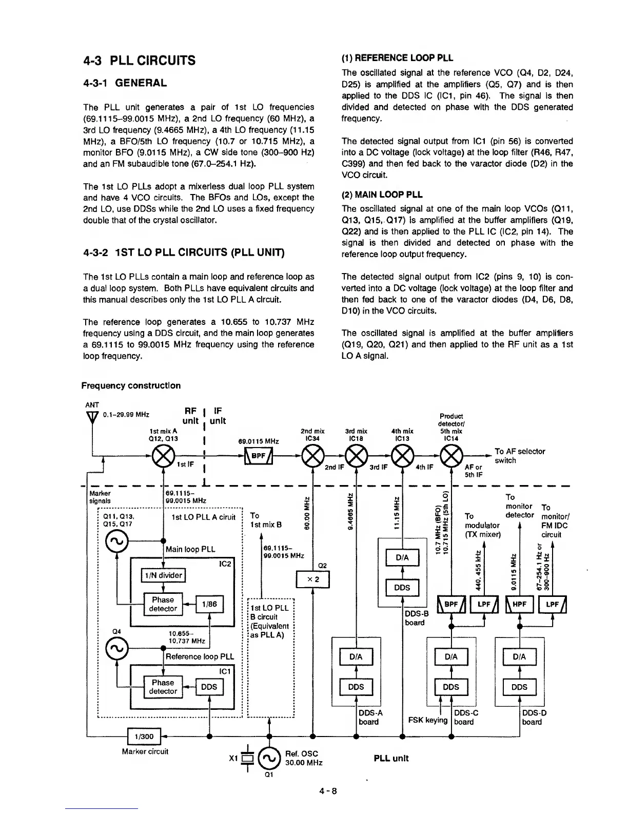
4-3
PLL CIRCUITS
4-3-1
GENERAL
The PLL unit
generates
a
pair of 1st LO
frequencies
(69.1115-99.0015
MHz),
a
2nd LO frequency
(60
MHz), a
3rd LO
frequency
(9.4665
MHz), a 4th LO
frequency
(11.15
MHz), a
BFO/5th LO
frequency
(10.7
or 10.715 MHz),
a
monitor BFO
(9.0115
MHz),
a
CW
side tone (300-900 Hz)
and
an FM
subaudible tone (67.0-254.1 Hz).
The 1st LO PLLs
adopt
a
mixerless dual loop PLL
system
and
have 4
VCO
circuits.
The
BFOs
and
LOs, except the
2nd
LO,
use DDSs
while the 2nd LO uses a fixed
frequency
double that of the
crystal oscillator.
4-3-2
1ST
LO
PLL CIRCUITS (PLL UNIT)
The
1st LO PLLs
contain a main loop and reference loop
as
a
dual
loop
system.
Both
PLLs have
equivalent
circuits
and
this manual describes only the 1 st LO PLL A
circuit.
The
reference loop
generates
a 10.655
to
10.737 MHz
frequency
using
a
DOS circuit, and the main loop generates
a 69.1115 to 99.0015 MHz
frequency using the reference
loop frequency.
(1)
REFERENCE LOOP PLL
The oscillated signal at the reference
VCO
(04,
D2, D24,
D25) Is
amplified
at
the amplifiers
(Q5, 07)
and
is
then
applied to the
DOS 1C (IC1,
pin
46).
The signal
is
then
divided and detected on phase with the DOS generated
frequency.
The detected signal output from IC1 (pin
56)
is converted
into
a DC
voltage (lock
voltage)
at the loop filter
(R46, R47,
C399)
and then fed back
to
the varactor diode
(D2)
in the
VCO
circuit.
(2)
MAIN LOOP PLL
The oscillated signal at one of the main loop VCOs
(01
1
,
013,
015,
017)
is
amplified at the buffer amplifiers
(019,
022)
and
is
then applied to the PLL
1C
(IC2, pin
14).
The
signal
is
then divided
and
detected
on
phase
with
the
reference loop output frequency.
The detected signal
output
from
IC2
(pins
9,
10)
is con-
verted
into a DC voltage (lock voltage) at the loop filter and
then
fed back to one of the varactor diodes (D4, D6, D8,
D1
0)
in
the
VCO
circuits.
The oscillated signal is amplified at the buffer amplifiers
(019, 020,
021)
and then applied
to
the RF unit
as a
1st
LO A
signal.
Frequency
construction
ANT
m
0.1-29.99
MHz
RF
unit
IF
unit
1st
mix A
Q12,
Q13
89.0115 MHz
2nd mix
tC34
3rd mix
IC18
4th mix
IC13
Product
detector/
5th mix
IC14
1st
IF
AF or
5th IF
To AF
selector
switch
Marker
signals
Q11,Q13,
Q15.
Q17
0^
89.1115-
199.0015 MHz
1st LO
PLL A
ciruit
X
s
To
1st mix B
Main loop PLL
IC2
1
/N
divider
Phase
detector
1/86
10.655-
10.737 MHz
69.1115-
99.0015
MHz
Q2
X
2
IstLO PLL
B
circuit
(Equivalent
as PLL
A)
D/A
DDS
Reference loop
PLL
IC1
Phase
detector
DOS
D/A
r:
DDS
LU
ru
1/300
DDS-A
board
o
K
u.
—
CD N
X
^
2
to
h**
6
d
To
modulator
(TX mixer)
To
monitor
detector
DDS-B
board
To
monitor/
FM IDC
circuit
.
O
O
to
»
CN
I
I O
O
«e>
CO
rn
D/A
DDS
m
FSK keying
LPF
j
D/A
‘
DDS
DDS-C
board
DDS-D
board
Marker circuit
XI
n
Ref. OSC
30.00 MHz
PLL unit
Q1
4-8