3 - 3
3-2 TRANSMITTER CIRCUITS
3-2-1 MICROPHONE AMPLIFIER CIRCUIT
(MAIN UNIT)
The microphone amplifier circuit amplifies audio signals
from the microphone, within +6 dB/octave pre-emphasis
characteristics (300 Hz–3 kHz), to a level needed for the
modulation circuit.
The AF signals from the microphone are applied to the
IN/EXT MIC switch (IC16, pin 7) via the “MIC” signal. When
using a headset, “EXTMIC” signal are applied to the exter-
nal switch (IC16, pin 6) via R336 to adjust the external
microphone level. The output signal from IC16 (pin 1) are
applied to the ALC amplifier (IC4, pin 9) via R110 to adjust
the microphone sensitivity.
The output signal from IC4 (pin 7) are amplified at the AF
amplifier (IC5), and then applied to the MOD/AF switch via
the high-pass filter (IC51) and low-pass filter (IC19) to filter
out RF components. The filtered signals are applied to the
modulation circuit.
3-2-2 MODULATION CIRCUIT (MAIN UNIT)
The modulation circuit modulates the VCO oscillating signal
(RF signal) using the microphone AF signal.
The audio signals are passed through the MOD/AF switch
(IC48, pin 6) via the modulation depth adjustment pot R121.
The signals are converted to the PWM wave form at the
PWM (Pulse-Width-Modulation) IC (IC44, pin 3), and power
amplified at the FET driver (IC47, pin 5) and power MOS
FET (Q92, Q93). The power-amplified signals are passed
through the line filter (L62–L64, L81, C456, C457, C462,
C463, C468), and then applied to the drain of power ampli-
fier (Q51) for the last stage modulation.
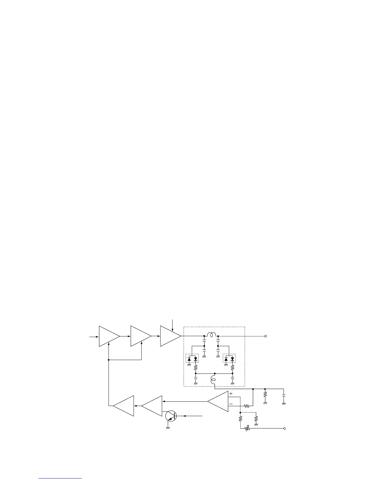
3-2-3 DRIVE/POWER AMPLIFIER CIRCUITS
(MAIN UNIT)
The amplifier circuit amplifies the VCO oscillating signal to
the output power level.
The signal from the buffer amplifiers (Q14, Q15) is passed
through the TX/RX switch (D11), and is amplified at the pre-
amplifier (Q42), pre-drivers (Q20, Q21) and the power
amplifier (Q51) to obtain 9 W of RF power.
The amplified signal is passed through the antenna swtich-
ing circuit (D3) and low-pass filter, and is then applied to the
antenna connector.
3-2-4 APC CIRCUIT (MAIN UNIT)
The APC (Automatic Power Control) circuit protects the
drive and power amplifiers from mismatched output loads.
The APC detector circuit (D4, D5) detects forward and
refrected signals respectively. The combined voltage is at a
minimum level when the antenna is matched at 50 Ω and is
increased when it is mismatched.
The detected voltage is applied to one of the APC controller
inputs (IC50, pin 3) and a power setting voltage is applied to
the other input (pin 1). When the antenna impedance is mis-
matched, the detected voltage exceeds the reference volt-
age. Thus the bias voltage of the pre-drivers is decreased.