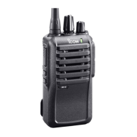
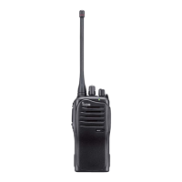
Do you have a question about the Icom IC-F4003 and is the answer not in the manual?
Detailed specifications including frequency range, channels, emission type, impedance, temperature, power, dimensions, weight, and IF.
Specifications for transmitter output power, modulation, frequency deviation, stability, emissions, and distortion.
Specifications for receiver sensitivity, squelch, intermodulation, spurious response, audio output, hum, noise, and selectivity.
Top-side view of the main circuit board, detailing component locations and labels.
Bottom-side view of the main circuit board, detailing component locations and labels.
Step-by-step instructions for safely removing the transceiver's chassis.
Step-by-step instructions for removing the main unit from the chassis.
Detailed explanation of the RF, 1st IF, and 2nd IF circuits involved in signal reception.
Description of the 2nd IF mixer, amplifier, and FM detector for demodulating the received signal.
Description of the 1st IF mixer, amplifier, and filtering stages in the receiver path.
Explanation of the audio frequency circuits for processing the received audio signal.
Overview of TX AF circuits, modulation, and TX amplifiers for transmitting signals.
Description of how the audio signal modulates the TX VCO for frequency modulation.
Explanation of the pre-amp, drive amp, and power amp stages in the transmitter.
Description of the VCOs, PLL IC, and frequency generation for transmit and receive.
Block diagram illustrating the power supply distribution across the transceiver's circuits.
Details pin assignments for CPU and D/A converter, outlining their functions.
Lists necessary equipment and initial setup steps for performing adjustments.
Details the required external connections for calibration and adjustment procedures.
Instructions for setting up cloning software and preparing adjustment channels.
Guide to using the software utility for fine-tuning transceiver parameters.
Procedures for adjusting PLL lock voltage and reference frequency for optimal performance.
Steps for adjusting TX output power, modulation balance, and frequency deviation.
Steps for adjusting receiver sensitivity and squelch threshold for clear reception.
List of mechanical components used in the transceiver's chassis with reference numbers.
List of optional accessories, part numbers, and their compatibility with the transceiver.
Diagram showing component placement and identification on the top of the main circuit board.
Diagram showing component placement and identification on the bottom of the main circuit board.
Part one of the voltage diagram for the main unit, illustrating voltage distribution.
Part two of the voltage diagram for the main unit, detailing voltage distribution and components.
| Brand | Icom |
|---|---|
| Model | IC-F4003 |
| Category | Transceiver |
| Language | English |