4 - 3
4-2-4 APC CIRCUIT
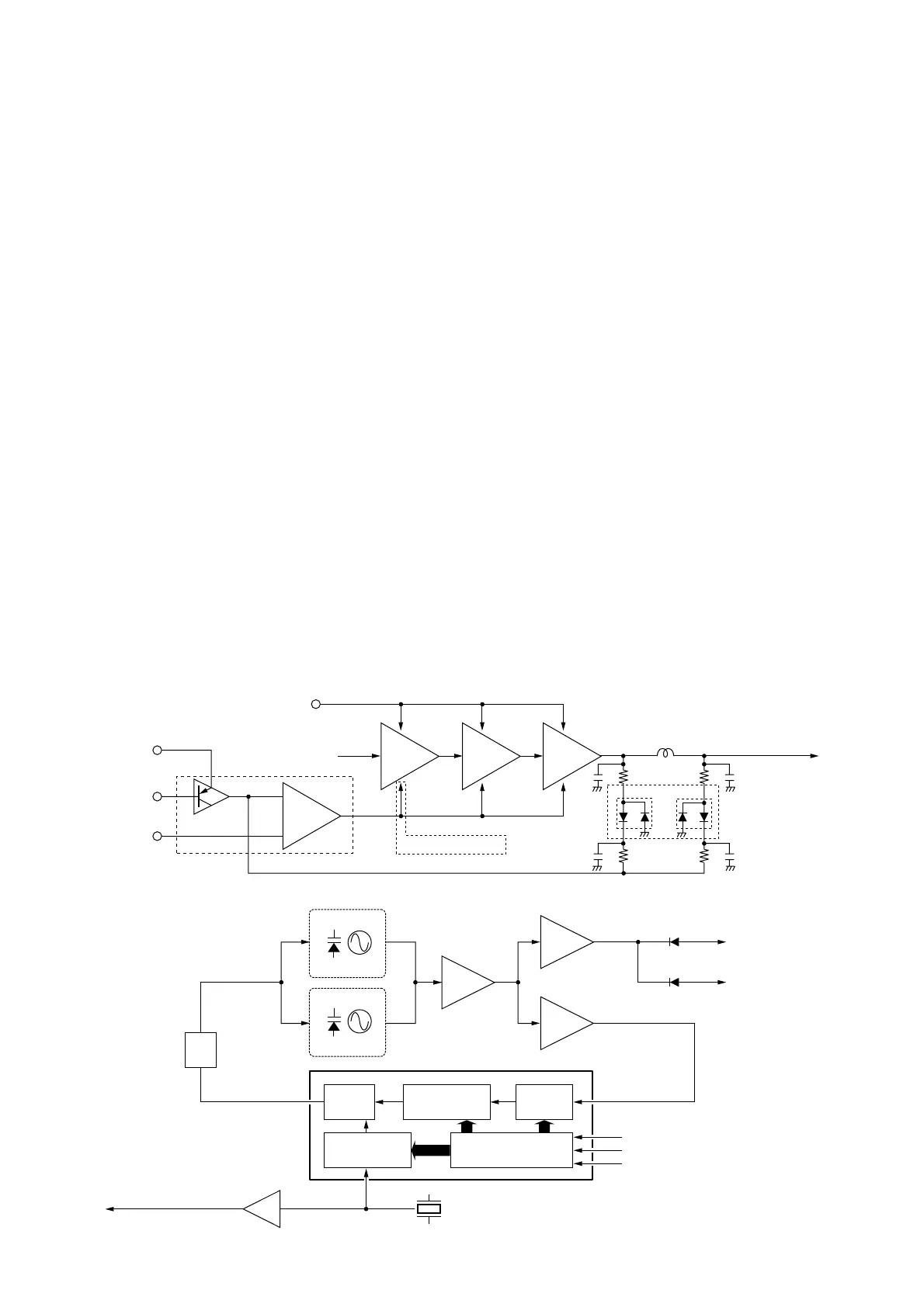
The APC circuit (IC4, Q22) protects the YGR (IC-F41GT/GS
only), drive and power amplifiers from excessive current
drive, and selects output power of HIGH, LOW2 or LOW1.
The APC detector circuit detects forward signals and reflec-
tion signals at D3 and D2 respectively. The combined volt-
age is at a minimum level when the antenna impedance is
matched at 50 Ω and is increased when it is mismatched.
The detected voltage is applied to the differential amplifier
(IC4, pin 3), and the “T4” signal from the D/A converter
(IC27, pin 4), controlled by the CPU (IC14), is applied to the
other input for reference. When antenna impedance is mis-
matched, the detected voltage exceeds the power setting
voltage. Then the output voltage of the differential amplifier
(IC4, pin 4) controls the input current of the YGR amplifer
(Q3; IC-F41GT/GS only), drive amplifier (Q2) and power
amplifier (Q1) to reduce the output power.
4-3 PLL CIRCUITS
4-3-1 PLL CIRCUIT
A PLL circuit provides stable oscillation of the transmit fre-
quency and receive 1st LO frequency. The PLL output com-
pares the phase of the divided VCO frequency to the refer-
ence frequency. The PLL output frequency is controlled by
the divided ratio (N-data) of a programmable divider.
The PLL circuit contains the TX/RX VCO circuit (Q12, Q11).
The oscillated signal is amplified at the buffer amplifiers (Q8,
Q7) and then applied to the PLL IC (IC1, pin 5).
The PLL IC contains a prescaler, programmable counter,
programmable divider and phase detector, etc. The entered
signal is divided at the prescaler and programmable counter
section by the N-data ratio from the CPU. The divided signal
is detected on phase at the phase detector using the refer-
ence frequency.
If the oscillated signal drifts, its phase changes from that of
the reference frequency, causing a lock voltage change to
compensate for the drift in the oscillated frequency.
4-3-2 VCO CIRCUIT
The VCO circuit contains a separate RX VCO (Q11, D6) and
TX VCO (Q12, D7, D8). The oscillated signal is amplified at
the buffer amplifiers (Q8, Q6) and is then applied to the T/R
switch (D5, D4). Then the receive 1st LO (Rx) signal is
applied to the 1st mixer (Q19) and the transmit (Tx) signal to
the YGR amplifier circuit (Q5).
A portion of the signal from the buffer amplifier (Q8) is fed
back to the PLL IC (IC1, pin 5) via the buffer amplifier (Q7)
as the comparison signal.
 Loading...