Do you have a question about the Icom IC-V80E and is the answer not in the manual?
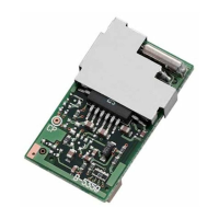
Component layout diagram for the top side of the main circuit board.
Component layout diagram for the bottom side of the main circuit board.
Procedure to remove the transceiver chassis, including antenna nut, knob, and screws.
Procedure to remove the main unit, including seals, nut, and unsoldering points.
Details the signal path for receiver circuits from antenna to IF stages.
Details the audio signal path from mic to VCO modulation and TX output.
Explains the VCO control, PLL operation, and frequency setting mechanisms.
Pin assignments for CPU (IC8) and D/A Converter (IC10) with their functions.
Lists essential equipment and their specifications for performing adjustments.
Procedure to access the adjustment mode by button combination during power-on.
Steps to calibrate the transceiver's frequency using external test equipment.
Procedure to adjust TX output power levels (High, Mid, Low) with RF power meter.
Steps to adjust RX sensitivity and Squelch levels.
Component layout diagram for the top side of the main circuit board.
Component layout diagram for the bottom side of the main circuit board.
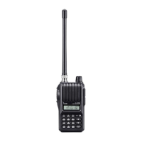
| Frequency Range | 136-174 MHz |
|---|---|
| Output Power | 5W |
| IP Rating | IP54 |
| Mode | FM |
| Antenna Connector | BNC |
| Operating Voltage | 7.2 V |
| MIL-STD | MIL-STD-810 |
| Channel Spacing | 25/12.5 kHz |
| Battery | Li-ion |