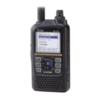
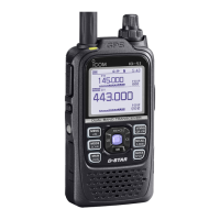
4 - 8
4-4 PORT ALLOCATIONS
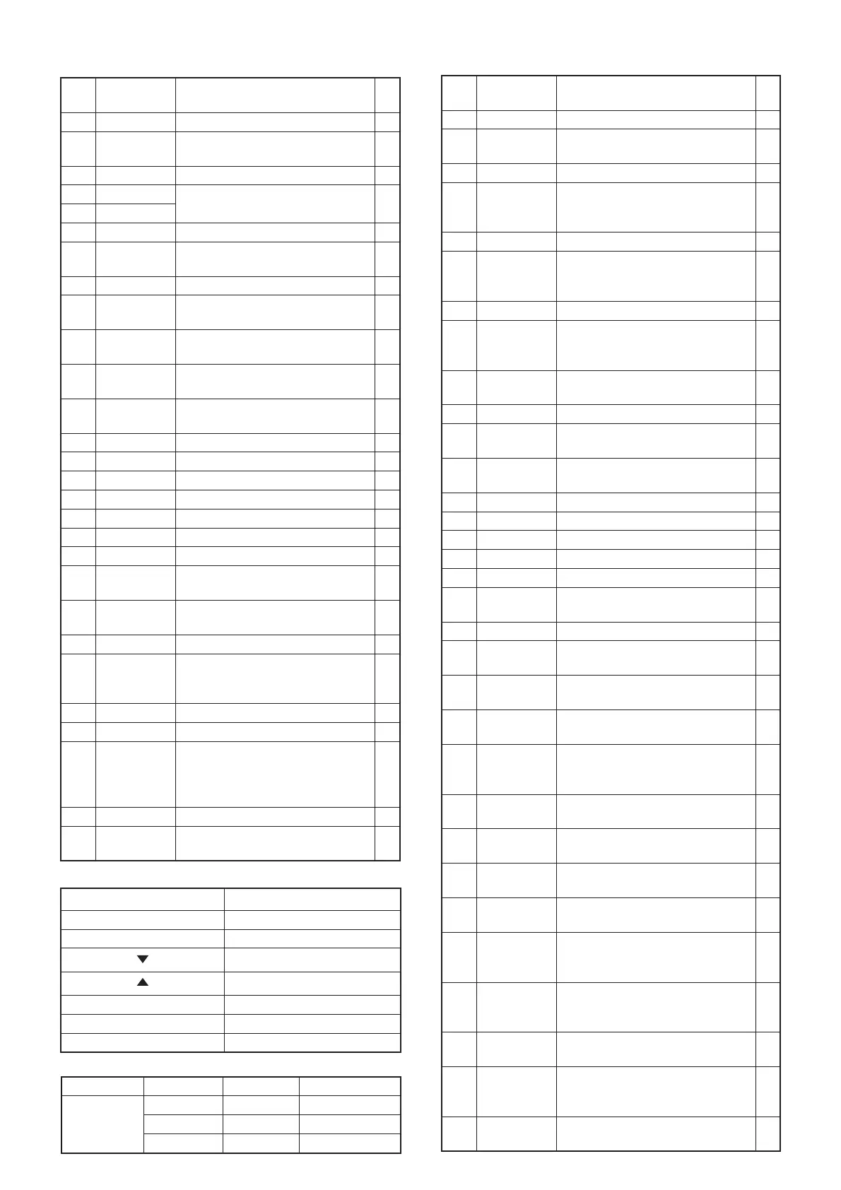
• CPU (LOGIC UNIT: IC5)
Pin
No.
Line Name Description I/O
A10 DICK1 [DIAL] (outer dial) (S12) phase-A I
A11 AUNLK
PLL unlock detection. (Band A)
L=Unlocked.
I
A12 DALD D/A converter serial strobe. O
A13 KS0
Key matrix strobe. O
A14 KS2
A4 BLV Lock voltage. (Band B) I
A5 REMOTE*
Key inputs from the external mi-
crophone.
I
A6 VIN External power supply voltage. I
A7 ATONE
WX alert signal (1050 Hz). (Band
A)
I
A8 TTEMP
TX power AMP temperature sens-
ing voltage.
I
A9 AUDI
Response signal from the audio
IC.
I
B1 DTMF
DTMF tone, european tone and
beep sound signals.
O
B10 DIUD1 [DIAL] (outer dial) (S12) phase-B I
B11 CLSFT1** CPU clock frequency shift control. O
B13 KS1 Key matrix strobe. O
B15 KR0 Key matrix return. I
B4 BRSSI RSSI voltage. (Band B) I
B5 ALV Lock voltage. (Band A) I
B7 TXI-V Transmit current sensing voltage. I
B8 TEMP
Charging circuit temperature sens-
ing voltage.
I
B9 AURES
Audio IC reset.
L=Reset.
O
C10 DIUD2 [DIAL] (inner dial) (S12) phase-B. I
C11 DTCS
TSQL/DTCS fi lter switching con-
trol.
H= While the DTCS tone is used.
O
C13 KS3 Key matrix strobe. O
C14 KR1 Key matrix return. I
C15 DCIN
External power supply connection
detect.
L= An external power supply is
connected.
I
C2 CTCSS CTCSS/DTCS tone signal. O
C4 BCTCIN
TSQL/DTCS tone signal. (Band
B)
I
Pin
No.
Line Name Description I/O
C5 VOX VOX sensing voltage. I
C7 ACTCIN
TSQL/DTCS tone signal. (Band
A)
I
C9 CLSFT2** Clock frequency shift control. O
D 1 DATA
Common serial clock to the PLL,
D/A converter, expander and au-
dio IC.
O
D10 DICK2 [DIAL] (inner dial) (S12) phase-A. I
D11 CK
Common serial clock to the PLL,
D/A converter, expander and au-
dio IC.
O
D12 KR2 Key matrix return. I
D13 BTDET
Battery type detection.
L= An appropriate battery pack is
attached.
I
D14 PWRSW
[POWER] key input.
L= Pushed.
I
D15 SCLK_R Radio IC serial clock. O
D2 G_RXD
UART data from the internal GPS
module.
I
D4 BTONE
WX alert signal (1050Hz). (Band
B)
I
D5 BTSENC Battery type detection. I
D6 BTVIN Battery voltage. I
D7 ARSSI RSSI voltage. (Band A) I
D8 AUSTB Audio IC serial strobe. O
D9 SEN_R Radio IC serial strobe. O
E13 RES_R
Radio IC reset.
L= Reset.
O
E14 SDIO_R Radio IC serial data. I/O
E4 G_TXD
UART data to the internal GPS
module.
O
F12 CHGC
Charging circuit control.
H= While charging.
O
F13 TXLED
TX LED control.
H= Lights.
O
F14 FMMUTE
RX AF mute control.
H= While receiving in the FM/FM-N
mode.
O
F15 BLED
Busy LED control.
H= Lights.
O
G12 INTMIC
MIC line switching control.
H= While the internal MIC is used.
O
G14 CHGH
Charging current control.
H= While charging using.
O
G15 PCON
Main power supply line control.
H= Power ON.
O
G3 LIGHT
LCD backlit and key backlit con-
trol.
H= Light.
O
G4 DIM
LCD backlit and key backlit bright-
ness control.
H= Bright.
O
H12 G_WKUP
GPS module wake-up control.
H= Power ON.
I
J1 BR3C
Receive circuit power control.
(Band B)
H= While receiving on band B.
O
J12 MMUTE
MIC mute control.
H= Mute.
O
**; Clock frequency shifting range.
Line name CLSFT1 CLSFT2 Shifting range
Line state
H H –1.2 kHz
HL
±0 kHz
L L ± 1.2 kHz
*; Key input sensing voltage.
Pushed key Voltage range
None of key is pushed. 2.698–3.300 V
VOX headset 2.216–2.468 V
[
]
1.708–2.213 V
[
]
1.283–1.705 V
A key 0.932–1.280 V
B key 0.637–0.928 V
Key locked. 0.000–0.634 V