2©2017 Integrated Device Technology, Inc. June 8, 2017
VersaClock
®
3S - 5P35023 Evaluation Board User Manual
Board Power Supply
Power Supply Options
The core voltage includes a digital voltage V
DD33
and an analog voltage V
DDA
. Both core voltages can be powered by USB as default.
▪ USB Power Supply only – When the board is connected to a PC through a USB cable, on-board voltage regulators will generate a
3.3V for the device. In this case, place the jumper as shown in Figure 2. See the JP5 jumper position for the on-board voltage
regulators in the following figure. USB power source is recommended because it's readily available right from your laptop.
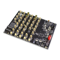
Table 1. Evaluation Board Labels and Functions
Label
Number
Name
On-board Connector
Label
Function
1 DIP Switch SW1
This is used to set outputs enable/disable on the IC and switches DFC
in different configurations.
2 Reference Output REF This is the reference or buffered output from the crystal.
3
Differential Clock Input CLKIN/CLKINB A differential clock can be connected as source for the device.
Single-ended Clock Input CLKINB
A Single-ended clock can be connected as source for the device using
CLKINB only.
4 Crystal, 25MHz This crystal is used as a reference source for the clock signal.
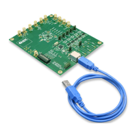
5 USB Connector J3 Connect this USB to your PC to run IDT Timing Commander.
A Differential Output #2 DIFF_T2/C2
This can be a differential pair, or two single-ended outputs. By default,
it’s an LPHCSL differential output.
B Output-enable Connector OE3 This port can be used in Pro-active Power Saving (PPS) mode.
C Single-ended Output SE_3
This is the single-ended output. By default it’s an LVCMOS
single-ended output.
D Differential Output #1 DIFF_T1/C1
This can be a differential pair, or two single-ended outputs. By default,
it’s LPHCSL differential output.
E Output-enable Connector SMA_OE1 This port can be used in Pro-active Power Saving (PPS) mode.
F Single-ended Output SE_1
This is the single-ended output. By default it’s an LVCMOS
single-ended output.
G Single-ended Output SE_2
This is the single-ended output. By default it’s an LVCMOS
single-ended output.
H Output enable Connector OE2 This port can be used in Pro-active Power Saving (PPS) mode.
I Output Voltage Selector E1, E2, E3, E4, E5
This is a four-way header used to select an output voltage. Connect
center pin to GND, and then the respective voltage (3.3V as default).
J Input Selector JP5, JP6 This is used to configure input from USB or external power supply.