User’s Manual 10 Rev. 1.0
2019-04-29
TLE5501
TMR-Based Angle Sensor
Connection to a micro controller
3 Connection to a micro controller
The following chapters give some hints which should be considered when the TLE5501 is connected to a
microcontroller.
3.1 Sigma-Delta ADC
In a Sigma-Delta ADC, the analog input signal is converted into a bit stream with the bit density corresponding
to the analog input value. The sampling frequency is much higher (~MHz) than the signal frequency. A
decimation filter converts the bit stream into a digital word (demodulation).
This type of ADC has typically a high input resistivity which makes it ideally suited for connection to a high
impedance current source. Very low input currents are drawn which do not influence the sensor output
voltage. Also, high resolution can be achieved which, however, comes together with a larger delay of the
signal.
Difficult for this type of ADC is the synchronization of the sine and cosine channel, which is mandatory to
achieve a high angle accuracy. To implement the proposed safety mechanisms for the TLE5501, it is also
required to sample the single ended signals SIN_P, SIN_N, COS_P, COS_N. This makes single ended ADC
channels necessary. The four channels should be sampled synchronous or with a very low time difference.
If the microcontroller in use allows to implement the above described requirements, a Sigma-Delta ADC is a
good choice for the connection to the TLE5501.
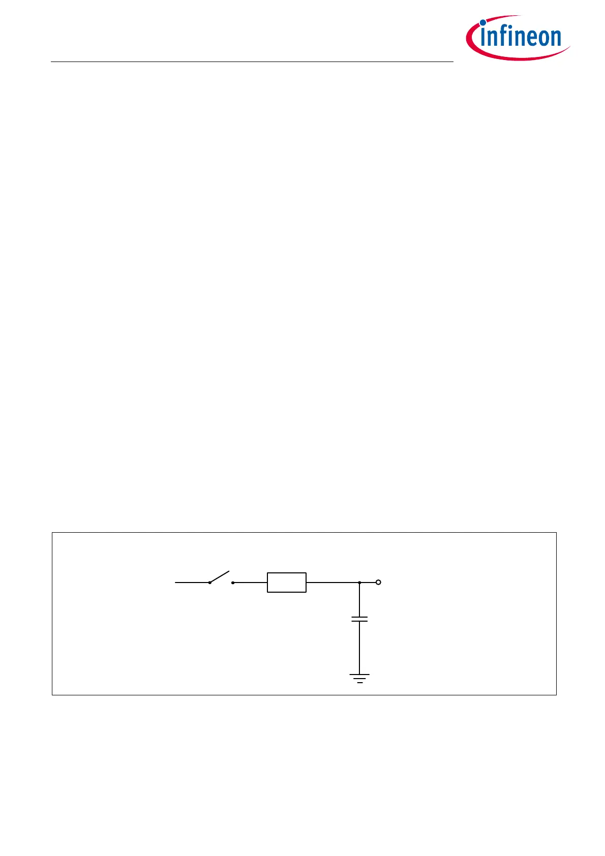
3.2 SAR ADC
The SAR (successive approximation register) is a widely used ADC and available on most micro controllers. Its
input is a switched capacitor structure with a sample and hold circuit. It supports a fast sampling frequency
with a typical resolution of 10 to 12 bits.
Figure 9 shows an input structure of an SAR ADC. In the “sample” phase, the S/H switch is closed and the
“sample and hold” capacitor C
SH
is charged via the resistor R
SH
(sampling time). After the sampling time the
switch S/H is opened and the voltage stored in C
SH
is converted to a digital value (hold time). The total time
required for charging the capacitor and conversion to a digital value is called conversion time.
Figure 9 Schematic input structure of an SAR ADC.
The high output impedance of the TMR bridge together with the external buffer capacitor C
b
has a
considerable impact on the timing behavior of the SAR ADC. An equivalent circuit is shown in Figure 10.
 Loading...