User Manual 3-3 V2.1
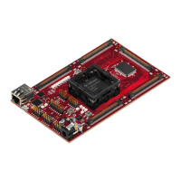
TriBoard TC3X9 TH V2.0(1) and TriBoard TC3X9 V2.0 2017-11
TriBoard Manual TC3X9
Hardware: TriBoard TC3X9 TH V2.0(1) and TriBoard TC3X9 V2.0
TriBoard Information
– D306 up to D309 (blue) -> toogle LEDs connected to P20.11 ... P20.14
– D504 RST (red) -> RESET LED indicate the reset state of the board (/ESR0)
– D505 +1V25 (green) -> +1V25 power supply indication
– D506 +3V3 (green) -> +3,3V power supply indication
– D507 V_UC (green) -> +5V/+3,3V power supply indication
– D508 SS2 (green) -> safe state signal 2 indication
– D402 ACT (green) -> on board miniWiggler JDS is ACTIV
– D401 RUN (blue) -> Debug RUN mode (switched by DAS Server)
3.5 Clock
On the board is a fixed crystal with 20MHz assembled. You can change this by replacing Y101 (soldered).
3.6 External Memory (only with TC399)
The TriBoard supports the following memory configurations:
• up to 4 MBytes external Burst Flash (1x32Bit) or
• up to 2 MBytes external asynchronous SRAM (2x16Bit) or
• up to 4 MBytes external synchronous SRAM (1x32Bit) or
• up to 1 MBytes external asynchronous SRAM (1x16Bit)
For the On Board Memory are reserved chip select 0 and 1. Therefore only two parts, e.g. 1x32Bit Flash and
2x16Bit asynchronous SRAM, should be assembled and can be used at the same time. Chip Select 2 is used as
Burst Address Advance output on the board and can be used externally only if the flash and the sysnchronous
SRAM (if assembled) are not used in burst mode.
3.6.1 External Flash (only with TC399)
The flash uses 32 Data Bits (AD0...AD31) and 20 Address Bits (A0...A19). It’s accessed via /CS0 or /CS1. The flash
has its own resistor to connect to /CS0 or /CS1. To connect the flash see Table 4-4.
Note: Only +3,3V Flash is usable with this board.
3.6.2 External SRAM (only with TC399)
The SRAM uses 32 Data Bits (AD0...AD31) and up to 20 Address Bits (A0...A19).
It’s accessed via /CS0 or /CS1. Each type of SRAM has its own resistor to connect to /CS0 or /CS1. To connect
different SRAMs see Table 4-4.
Note: Only +3,3V SRAM is usable with this board.
3.7 USB Connector
The USB connector is used for connection to a PC. Via the USB it is possible to power the board, using the ASCLIN0
as serial connection via USB and Debugging via DAS. For the pinout of USB socket see Figure 6-5.
NOTE: Before connecting the board to the PC, make sure that the actual DAS software is installed on the PC. For
actual DAS software please contact your local FAE.
The software can also be found on:
DAS website
 Loading...