80960KB
13
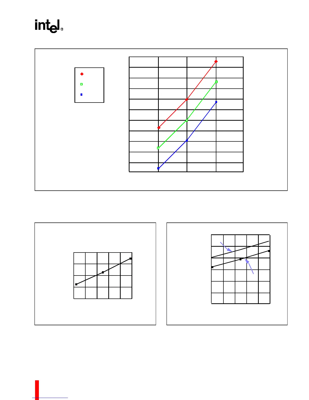
Figure 9. Typical Current vs. Frequency (Hot Temp)
OPERATING FREQUENCY (MHz)
@4.5V
@5.0V
@5.5V
TYPICAL SUPPLY CURRENT (mA)
TEMP = +22°C
380
360
340
320
300
280
260
240
220
200
180
16 20 25
160
Figure 10. Worst-Case Voltage vs. Output
Current on Open-Drain Pins
Figure 11. Capacitive Derating Curve
2.5 Test Load Circuit
Figure 12 illustrates the load circuit used to test the
80960KB’s three-state pins; Figure 13 shows the
load circuit used to test the open drain outputs. The
open drain test uses an active load circuit in the form
01020304050
0.8
0.6
0.4
0.2
0.0
OUTPUT LOW CURRENT(mA)
(TEMP = +85°C, V
CC
= 4.5V)
OUTPUT LOW VOLTAGE (V)
020406080100
30
25
20
15
10
CAPACITIVE LOAD(pF)
(TEMP = +85°C, V
CC
= 4.5V)
5
0
RISING
FALLING
VALID DELAY(ns)
THREE-STATE OUTPUT