80960KB
15
2.7 DC Characteristics
2.6 Absolute Maximum Ratings
NOTICE:This is a production data sheet. The specifi-
cations are subject to change without notice.
Operating Temperature(PGA)................... 0°C to +85°C Case
(PQFP)............. 0°C to +100°C Case
Storage Temperature.................................... –65°C to +150°C
Voltage on Any Pin .................................. –0.5V to VCC +0.5V
Power Dissipation............................................ 2.5W (25 MHz)
*WARNING: Stressing the device beyond the
“Absolute Maximum Ratings” may cause
permanent damage. These are stress ratings
only. Operation beyond the “Operating Condi-
tions” is not recommended and extended
exposure beyond the “Operating Conditions” may
affect device reliability.
PGA: 80960KB (16 MHz) T
CASE
= 0°C to +85°C, V
CC
= 5V ± 10%
80960KB (20 and 25 MHz) T
CASE
= 0°C to +85°C, V
CC
= 5V ± 5%
PQFP: 80960KB (16 MHz) T
CASE
= 0°C to +100°C, V
CC
= 5V ± 10%
80960KB (20 and 25 MHz) T
CASE
= 0°C to +100°C, V
CC
= 5V ± 5%
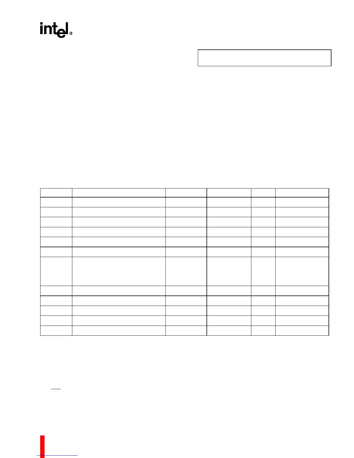
Table 6. DC Characteristics
Symbol Parameter Min Max Units Notes
V
IL
Input Low Voltage –0.3 +0.8 V
V
IH
Input High Voltage 2.0 V
CC
+ 0.3 V
V
CL
CLK2 Input Low Voltage –0.3 +0.8 V
V
CH
CLK2 Input High Voltage 0.55 V
CC
V
CC
+ 0.3 V
V
OL
Output Low Voltage 0.45 V (1,2)
V
OH
Output High Voltage 2.4 V (3,4)
I
CC
Power Supply Current:
16 MHz
20 MHz
25 MHz
315
360
420
mA
mA
mA
(5)
(5)
(5)
I
LI
Input Leakage Current ±15 µA 0 ≤ V
IN
≤ V
CC
I
LO
Output Leakage Current ±15 µA 0.45 ≤ V
O
≤ V
CC
C
IN
Input Capacitance 10 pF f
C
= 1 MHz (6)
C
O
Output Capacitance 12 pF f
C
= 1 MHz (6)
C
CLK
Clock Capacitance 10 pF f
C
= 1 MHz (6)
NOTES:
1. For three-state outputs, this parameter is measured at:
Address/Data ........................................ 4.0 mA
Controls.................................................. 5.0 mA
2. For open-drain outputs ........................... 25 mA
3. This parameter is measured at:
Address/Data ...................................... -1.0 mA
Controls................................................ -0.9 mA
ALE
..................................................... -5.0 mA
4. Not measured on open-drain outputs.
5. Measured at worst case frequency, V
CC
and temperature, with device operating and outputs loaded to the test conditions
in Figures 12 and 13. Figure 7, Figure 8 and Figure 9 indicate typical values.
6. Input, output and clock capacitance are not tested.