16
80960KB
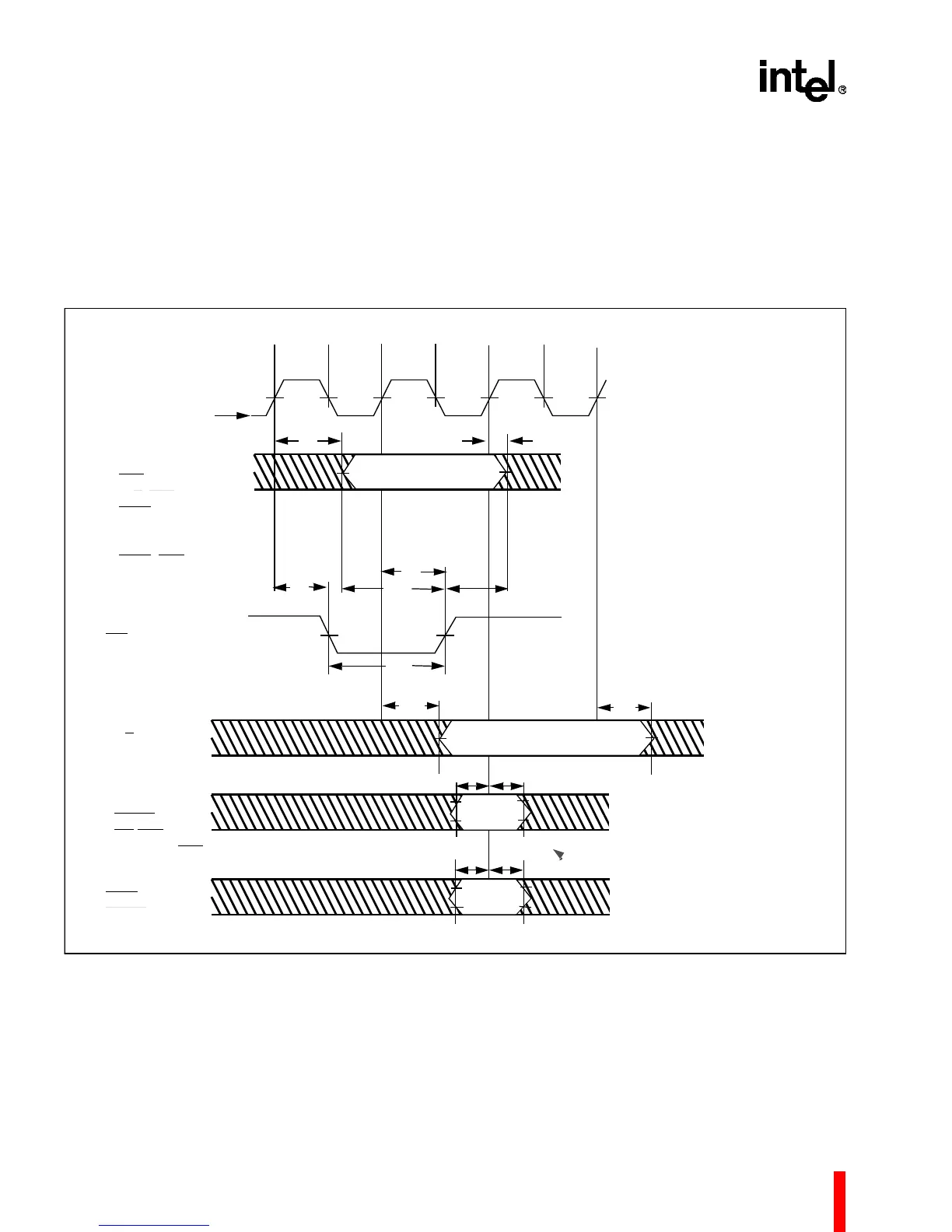
2.8 AC Specifications
This section describes the AC specifications for the
80960KB pins. All input and output timings are
specified relative to the 1.5 V level of the rising edge
of CLK2. For output timings the specifications refer
to the time it takes the signal to reach 1.5 V.
For input timings the specifications refer to the time
at which the signal reaches (for input setup) or
leaves (for hold time) the TTL levels of LOW (0.8 V)
or HIGH (2.0 V). All AC testing should be done with
input voltages of 0.4 V and 2.4 V, except for the
clock (CLK2), which should be tested with input
voltages of 0.45 V and 0.55 V
CC
.
Figure 14. Drive Levels and Timing Relationships for 80960KB Signals
ABC
D
A
BC
1.5V
1.5V 1.5V 1.5V
0.8V
T
6
1.5V
1.5V
T
7
1.5V
1.5V
VALID OUTPUT
T
6
T
8
T
8
T
13
T
14
1.5V 1.5V
VALID OUTPUT
T
9
2.0V 2.0V
2.0V 2.0V
0.8V 0.8V
0.8V 0.8V
EDGE
CLK2
OUTPUTS:
LAD 31:0
ADS
W/R, DEN
BE3:0
HLDA
CACHE
LOCK, INTA
ALE
DT/R
INPUTS:
LAD31:0
BADAC
IAC/INT0, INT1
INT2/INTR, INT3
HOLD
LOCK
READY
T
9
VALID INPUT
T
10
T
11
T
12
T
11