Page 40 © JVA Technologies Pty. Ltd. www.jva-fence.com
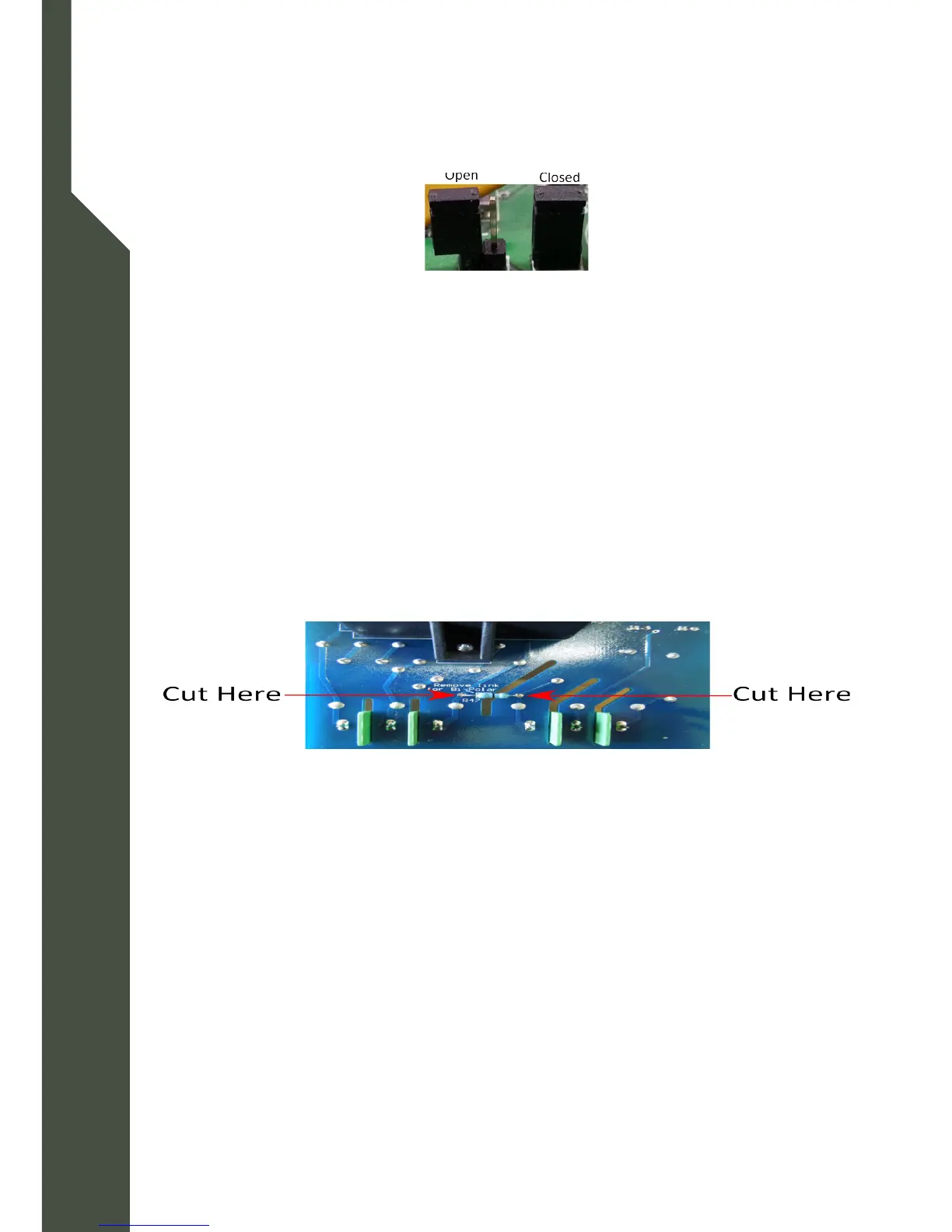
7.3.1
diagram below.
Step 1
On the back of the Z14/R PCB near the high voltage output terminals there