1-32
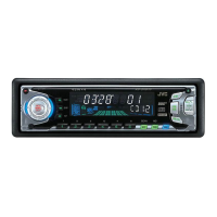
KD-SX8250/KD-SX780
109876
12345
CONTROL
CIRCUIT
LVref
RVref
LOGIC
CIRCUIT
CONTROL
CIRCUIT
CCB
INTERFACE
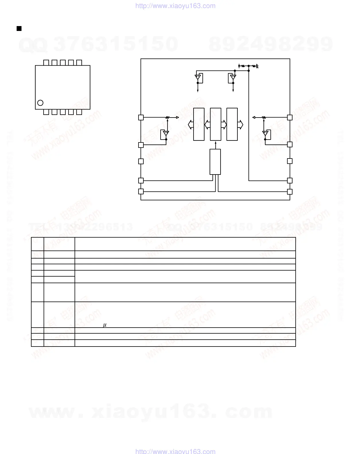
LC75344M-X(IC252):Sub woofer
1.Terminal layout
3.Pin function
2.Block diagram
12345
109876
Pin
No.
1
2
3
4
5
6
7
8
9
10
LIN
LOUT
VDD
DI
CL
CE
Vref
VSS
ROUT
RIN
Input signal connections
Volume output
Power supply
Serial data and clock inputs used for IC control
Chip enable
Data is writen to the internal latch when this pin goes from high to low. The internal
analog switches operate at this point. Data transfer is enabled when this pin is high.
Connection to the 0.5 x VDD voltage generator circuit used as the analog signal
ground.
To a power supply ripple countermeasure,application must connect a capacitor of
about 10 F between this pin and AVSS(VSS).
Ground
Volume output
Input signal connections
Symbol Function
w
w
w
.
x
i
a
o
y
u
1
6
3
.
c
o
m
Q
Q
3
7
6
3
1
5
1
5
0
9
9
2
8
9
4
2
9
8
T
E
L
1
3
9
4
2
2
9
6
5
1
3
9
9
2
8
9
4
2
9
8
0
5
1
5
1
3
6
7
3
Q
Q
TEL 13942296513 QQ 376315150 892498299
TEL 13942296513 QQ 376315150 892498299
http://www.xiaoyu163.com
http://www.xiaoyu163.com
 Loading...