1-37
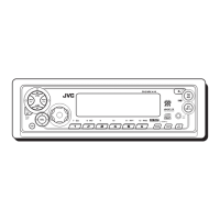
KD-SX8250/KD-SX780
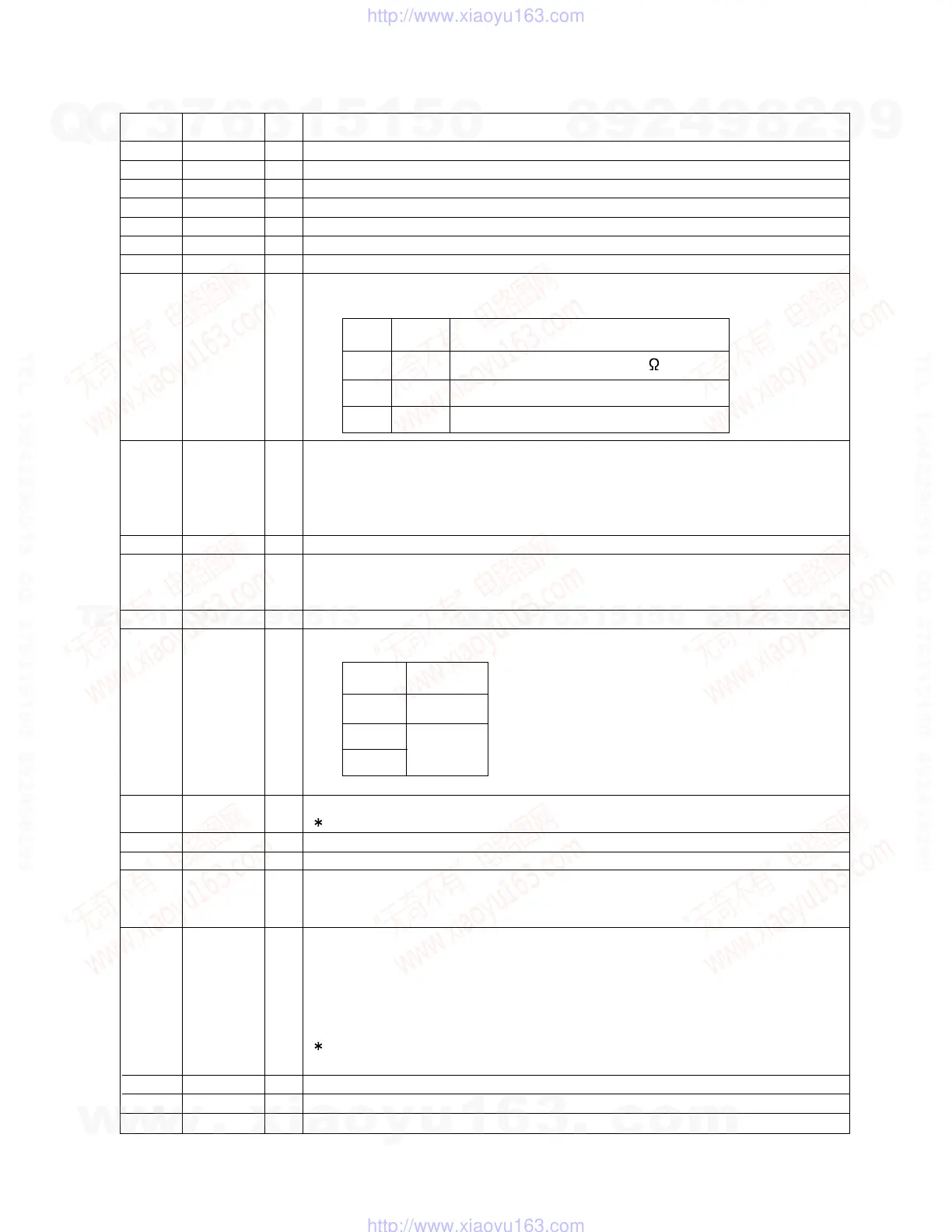
3.Pin function
Pin No. Symbol I/O Function
1
2
3
4
5
6
7
8
9
10
11
12
13
14
15
16
17
18
19
20
21
22
23
24
-
I
I
I
I
I
O
I
I
I
O
O
I
O
O
I
O
I
O
I
I
O
I
-
VCC
FNI
FPI
TPI
TNI
MDI
LDO
SEL
TEBC
TEN
TEO
RFDC
GVSW
VRO
FEO
FEN
RFRP
RFRPIN
RFGO
RFGC
AGCIN
RFO
RFN
GND
3.3V power supply pin
Main-beam amp input pin
Main-beam amp input pin
Sub-beam amp input pin
Sub-beam amp input pin
Monitor photo diode amp input pin
Laser diode amp output pin
APC circuit ON/OFF control signal, laser diode (LDO) control signal input
or bottom/peak detection frequency change pin.
Tracking error balance adjustment signal input pin
Adjusts TE signal balance by ellminating carrier component from PWM
signal (3-state output,PWM carrier = 88.2kHz) output from TC94A14F/FA
TEBC pin using RC-LPF and inputting DC.
TEBC input voltage:GND~VCC
Tracking error signal genaration amp negative-phase input pin
Tracking error signal generation amp output pin.
Combining TEO signal RFRP signal with TC94A14F/FA configures tracking
search system.
RF signal peak detection output pin
AGC/FE/TE amp gain change pin
Reference voltage (VRO) output pin
VRO=1/2VCC When VCC=3.3V
Focus error signal generation amp output pin
Focus error signal generation amp negative-phase input pin
Signal amp output pin for track count
Combining RFRP signal and TEO signal with TC94A14F/FA configures
tracking search system.
Signal generation amp input pin for track count
RF signal amplitude adjustment amp output pin
RF amplitude adjustment control signal input pin
Adjusts RF signal amplitude by eliminating carrier component from PWM
signal (3-state output,PWM carrier=88.2kHz)output fromTC94A14F/14FA
RFGC pin using RC-LPF and inputting DC.
RFGC input voltage:GND~VCC
RF signal amplitude adjustment amp input pin
RF signal generation amp output pin
RF signal generation amp input pin
GND pin
TA2175FN-X
SEL
GND
Hiz
VCC
VCC
APC
circuit
LCD
OFF Connected VCC through 1k resistor
ON
Control signal output
ON Control signal output
GVSW Mode
GND
Hiz
CD-RW
Normal
w
w
w
.
x
i
a
o
y
u
1
6
3
.
c
o
m
Q
Q
3
7
6
3
1
5
1
5
0
9
9
2
8
9
4
2
9
8
T
E
L
1
3
9
4
2
2
9
6
5
1
3
9
9
2
8
9
4
2
9
8
0
5
1
5
1
3
6
7
3
Q
Q
TEL 13942296513 QQ 376315150 892498299
TEL 13942296513 QQ 376315150 892498299
http://www.xiaoyu163.com
http://www.xiaoyu163.com
 Loading...