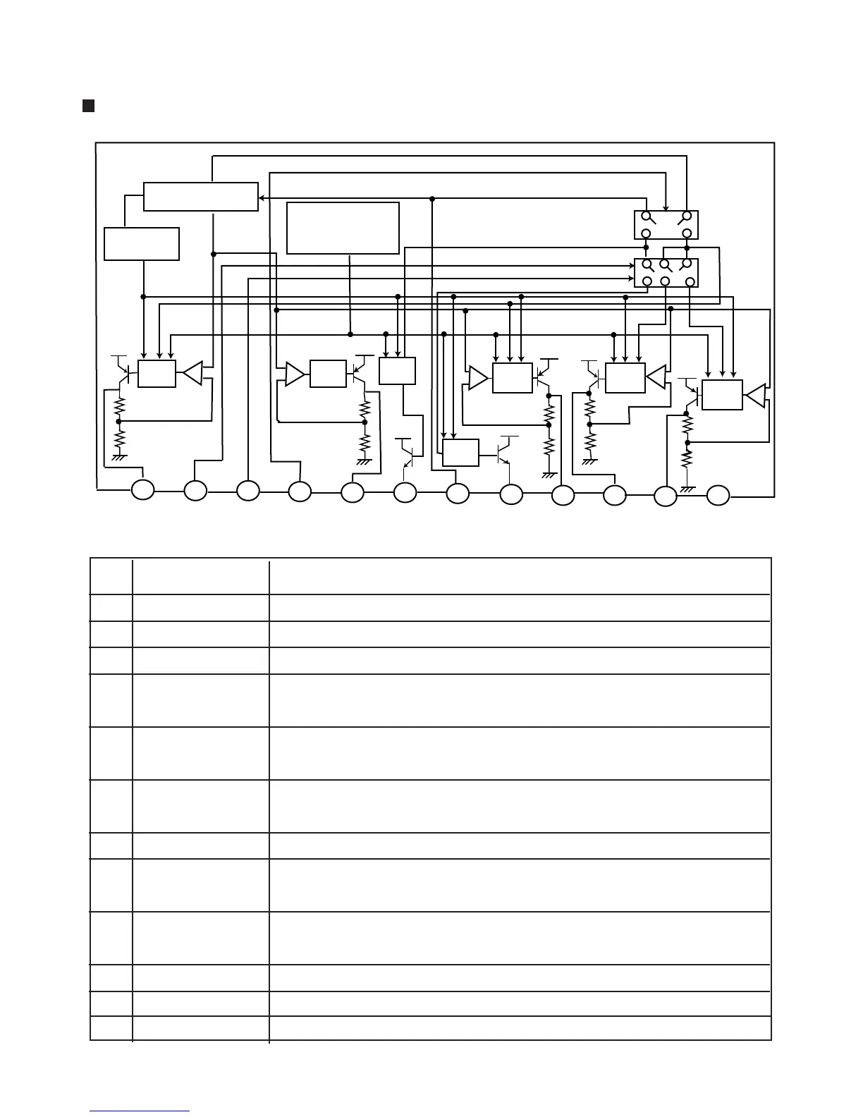
AN80T05LF (IC961) : Regulator
1. Block diagram
-
+
-
+
-
+
-
+
-
+
ILL
10V
MODE2 MODE1
STB
VDD
VCC
5.6V
AMP
ANT
COM
8.7V
8.7V
8.7V
AM
FM
GND
Reference Voltage
ASO & Peak
Current Protection
Thermal
Protection
Pre
Drive
Pre
Drive
Pre
Drive
Pre
Drive
Pre
Drive
AMT
Out
AMT
Out
1
2
3
4
5 6
7
8
9
10 11 12
2.Pin Function
Illumination output
MODE2 SW
MODE1 SW
STAND BY
VDD output
AMP output
VCC
ANT output
COM output
AM output
FM output
GND
1
2
3
4
5
6
7
8
9
10
11
12
10V power supply with a maximum output current of 300mA for a illumination.
AM and ANT output are turned ON when this pin is 5V.
AM and FM output are switched when this pin is 5V.
Only VDD output during the 0V standby state; ILL,COM and AMPoutputs
are turuned ON when this pin is 5V.
5.6V Power supply with amaximum output current of 100mA for a micro-
controiler. Output is always available if BACKUP power supply is connected.
Power supply to activate a remote amplfier; a voltage of about 1V(typ) lower
than VCC voltage is provided with a maximum output current of 500mA.
Connected to car BACKUP and ACC Power supplioes.
Power supply to drive an antenna voltage of about 1V(Tpy) lower than the VCC
voltage is provided with amaximum output current of 500mA.
8.7V power supply with a maximum output current of 150mA; this can be used
as a system common power supply.
8.7V power supply with a maximum output current of 150mV for AM receiver.
8.7V power supply with a maximum output current of 150mV for FM receiver.
Connected to the IC substrate.
Function
Pin name
Pin
No.
Description of major ICs
 Loading...