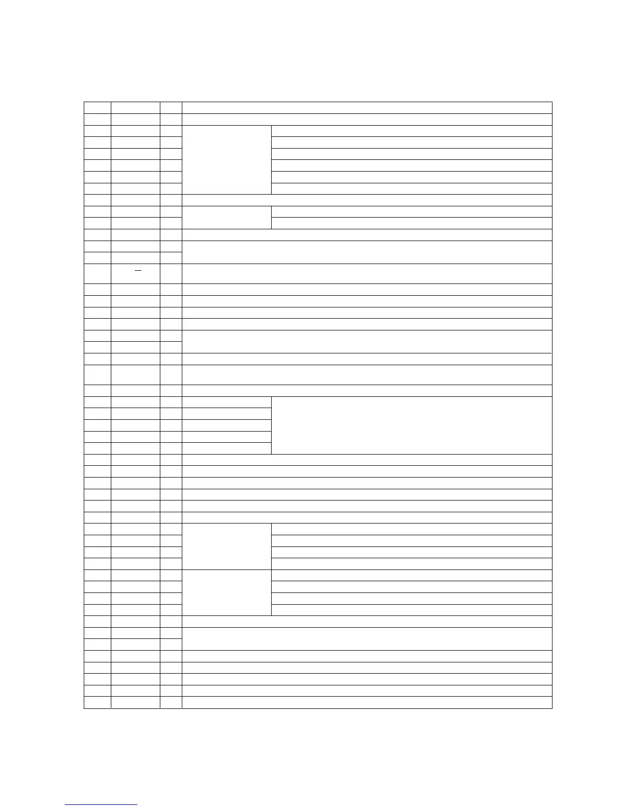
Pin No. Symbol I/O Function
1 DEFI I Defect detection signal (DEF) input. (Must be connected to 0 V when unused.)
2 TAI I Test input. A pull-down resistor is built in. Must be connected to 0 V.
3 PDO O External VCO control phase comparator output
4 VV
SS
Ð
PLL pins
Internal VCO ground. Must be connected to 0 V.
5 ISET AI PDO output current adjustment resistor connection
6 VV
DD
Ð Internal VCO power supply
7 FR AI VCO frequency range adjustment
8 V
SS
Ð Digital system ground. Must be connected to 0 V.
9 EFMO O
Slice level control
EFM signal output
10 EFMIN I EFM signal input
11 TEST2 I Test input. A pull-down resistor is built in. Must be connected to 0 V.
12 CLV
+
O
Disc motor control output.
13 CLV
Ð
O Three-value output is also possible when specified by microprocessor command.
14 V/P O
Rough servo/phase control automatic switching monitor output. Outputs a high level during rough servo and a low level
during phase control.
15 HFL I Track detection signal input. This is a Schmitt input.
16 TES I Tracking error signal input. This is a Schmitt input.
17 TOFF O Tracking off output
18 TGL O Tracking gain switching output. Increase the gain when low.
19 JP
+
O
Track jump output.
20 JP
Ð
O Three-value output is also possible when specified by microprocessor command.
21 PCK O EFM data playback clock monitor. Outputs 4.3218 MHz when the phase is locked.
22 FSEQ O
Synchronization signal detection output. Outputs a high level when the synchronization signal detected from the EFM
signal and the internally generated synchronization signal agree.
23 V
DD
Ð Digital system power supply.
24 CONT1 I/O General-purpose I/O pin 1
25 CONT2 I/O General-purpose I/O pin 2
Controlled by serial data commands from the microprocessor. Any of these that are unused
26 CONT3 I/O General-purpose I/O pin 3 must be either set up as input ports and connected to 0 V, or set up as output ports and
27 CONT4 I/O General-purpose I/O pin 4
left open.
28 CONT5 I/O General-purpose I/O pin 5
29 EMPH O De-emphasis monitor pin. A high level indicates playback of a de-emphasis disk.
30 C2F O C2 flag output
31 DOUT O Digital output. (EIAJ format)
32 TEST3 I Test input. A pull-down resistor is built in. Must be connected to 0 V.
33 TEST4 I Test input. A pull-down resistor is built in. Must be connected to 0 V.
34 N.C. Ð Unused. Must be left open.
35 MUTEL O Left channel mute output
36 LV
DD
Ð
Left channel
Left channel power supply
37 LCHO O one-bit D/A converter Left channel output
38 LV
SS
Ð Left channel ground. Must be connected to 0 V.
39 RV
SS
Ð Right channel ground. Must be connected to 0 V.
40 RCHO O
Right channel
Right channel output
41 RV
DD
Ð one-bit D/A converter Right channel power supply
42 MUTER O Right channel mute output
43 XV
DD
Ð Crystal oscillator power supply.
44 X
OUT
O
Connections for a 16.9344 crystal oscillator element
45 X
IN
I
46 XV
SS
Ð Crystal oscillator ground. Must be connected to 0 V.
47 SBSY O Subcode block synchronization signal output
48 EFLG O C1, C2, single and double error correction monitor pin
49 PW O Subcode P, Q, R, S, T, U, V and W output
50 SFSY O Subcode frame synchronization signal output. This signal falls when the subcodes are in the standby state.
LC78622 Pin Functions
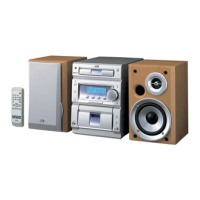
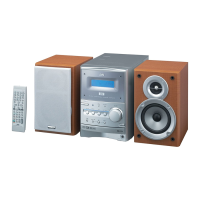
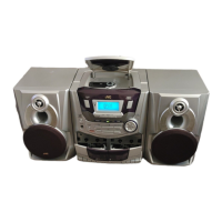
PC-X250
1 - 18
 Loading...