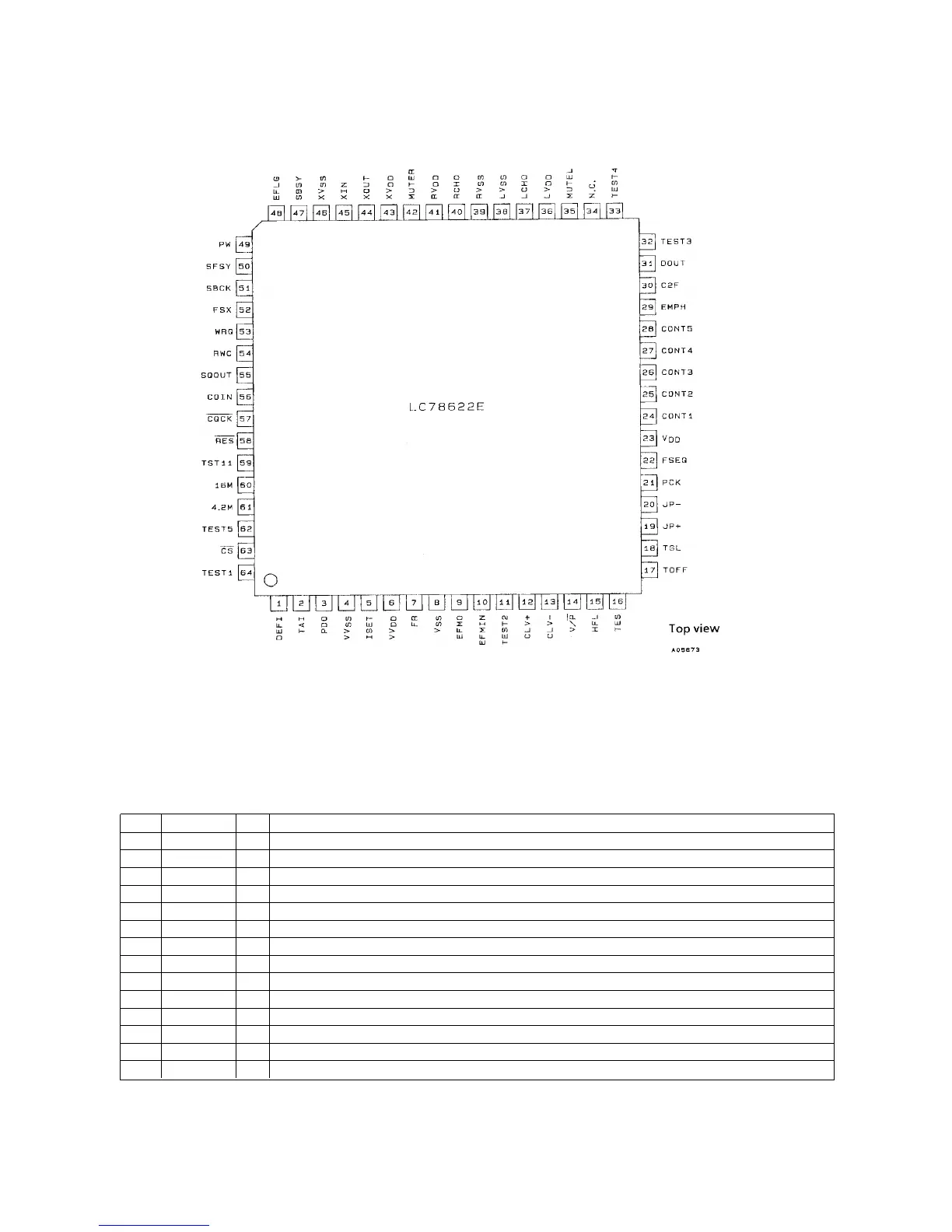
LC78622 Pin Function
Note: The same potential must be supplied to all power supply pins, i.e., V
DD
, VV
DD
, LV
DD
, RV
DD
, and XV
DD
.
Pin No. Symbol I/O Function
51 SBCK I Subcode readout clock input. This is a Schmitt input. (Must be connected to 0 V when unused.)
52 FSX O Output for the 7.35 kHz synchronization signal divided from the crystal oscillator
53 WRQ O Subcode Q output standby output
54 RWC I Read/write control input. This is a Schmitt input.
55 SQOUT O Subcode Q output
56 COIN I Command input from the control microprocessor
57 CQCK I Input for both the command input clock and the subcode readout clock. This is a Schmitt input.
58 RES I Chip reset input. This pin must be set low briefly after power is first applied.
59 TST11 O Test output. Leave open. (Normally outputs a low level.)
60 16M O 16.9344 MHz output.
61 4.2M O 4.2336 MHz output
62 TEST5 I Test input. A pull-down resistor is built in. Must be connected to 0 V.
63 CS I Chip select input. A pull-down resistor is built in. Must be connected to 0 V if not controlled.
64 TEST1 I Test input. No pull-down resistor. Must be connected to 0 V.
LC78622 Pin Assignment
PC-X250
1 - 17
 Loading...